Organic light emitting device pixel circuit and driving method therefor

a light-emitting device and circuit technology, applied in the field of flat-panel display, can solve the problems of difficult to manufacture transistors in the amoled, display non-uniformity, and difficulty in charging a data line, and achieve the effect of high-gradation representation

Active Publication Date: 2005-01-27
SAMSUNG DISPLAY CO LTD
View PDF5 Cites 197 Cited by
  • Summary
  • Abstract
  • Description
  • Claims
  • Application Information

AI Technical Summary

Benefits of technology

[0024] Yet still further in accordance with the present invention a pixel circuit in an organic light emitting device is provided capable o...

Problems solved by technology

Although this AMOLED has an advantage in that power consumption is low, current intensity flowing through the EL element changeing over time, causing display nonuniformity, can be a problem.
Since the threshold voltage of a thin film transistor for the driving transistor changes depending on manufacturing process parameters, it becomes difficult to manufacture transistors in the AMOLED so that all of the transistors have the same threshold voltage.
However, the organic light emitting device as described above employs a current driving approach for driving the EL element which depends on a data signal current level applied from the current source and has difficulty in charging a data line.
Because a parasitic capacitance of the data line is relatively larger while the current level of the data signal provided from the current source is relatively smaller, t...

Method used


Image

  • Organic light emitting device pixel circuit and driving method therefor
  • Organic light emitting device pixel circuit and driving method therefor
  • Organic light emitting device pixel circuit and driving method therefor

Examples


Embodiment Construction

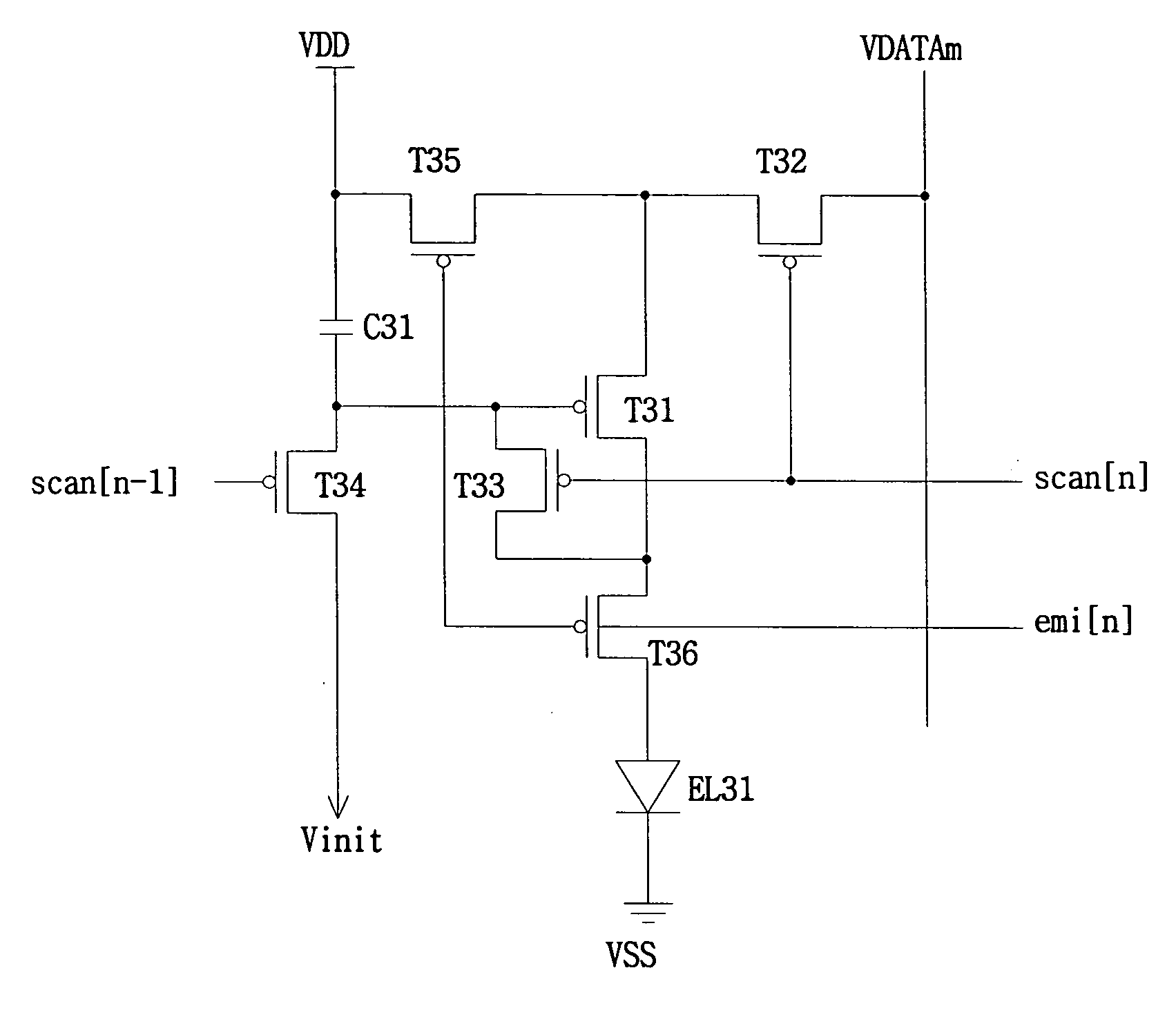
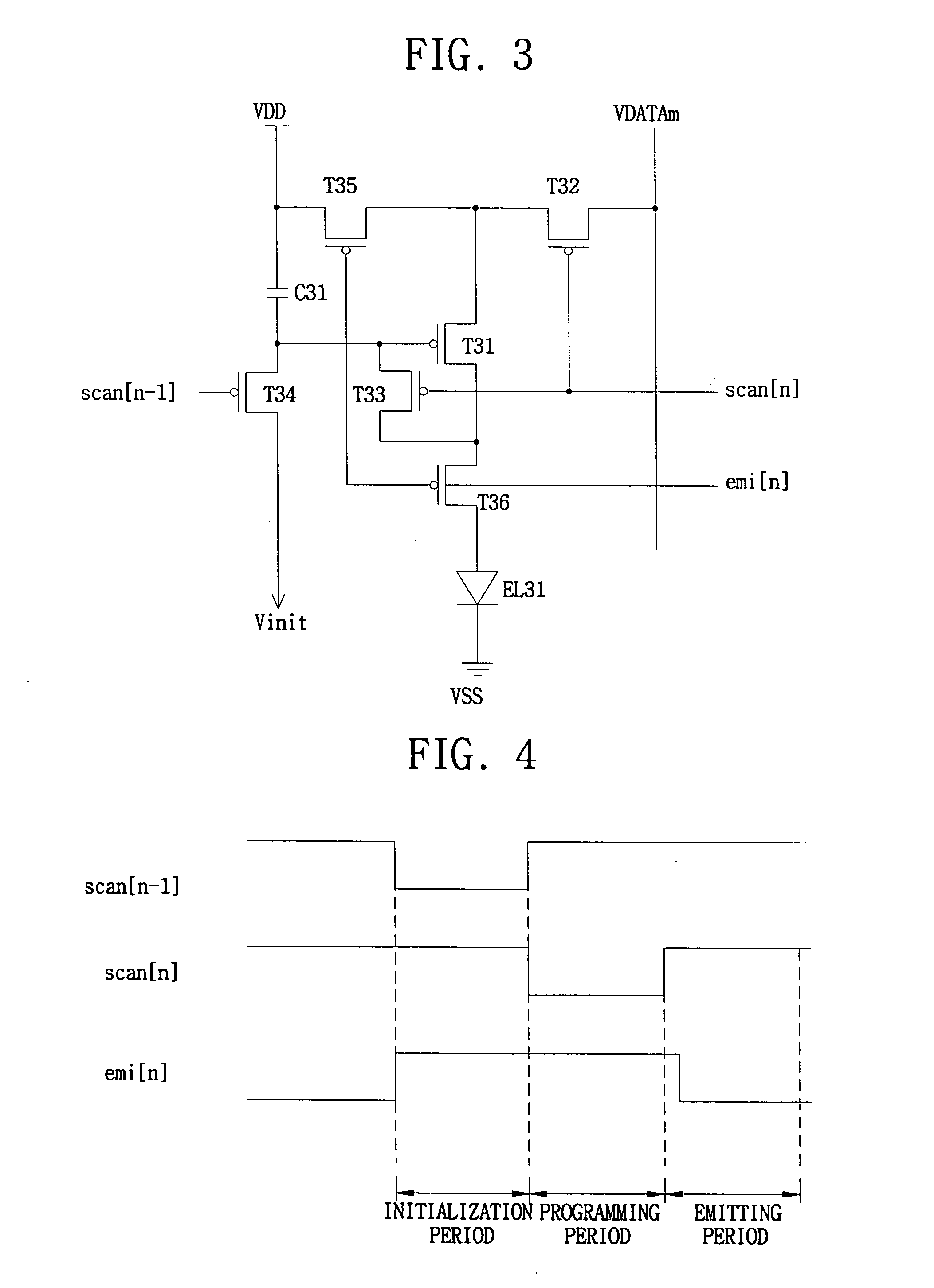
[0037] The organic light emitting device in accordance with the present invention includes a plurality of gate lines; a plurality of data lines; a plurality of power lines; and a plurality of pixels each arranged in an associated gate line, data line and power line of the plurality of gate lines, data lines and power lines. FIG. 3 shows only one pixel arranged in an associated gate line (the n-th gate line), data line (the m-th data line) and power line (the m-th power line).

[0038] Referring to FIG. 3, each pixel in the organic light emitting device according to the present invention is composed of six transistors T31-T36, one capacitor C31 and electroluminescent (EL) element EL31. That is, each pixel includes organic electroluminescent device EL31 for emitting light corresponding to an applied driving current; first switching transistor T32 for switching data signal voltage VDATAm, applied to the associated data line, in response to current scan line signal SCAN[n] applied to the ...


PUM


Abstract

A pixel circuit in an organic light emitting device capable of realizing high gradation representation by self-compensating a threshold voltage, and a method for driving the same. The pixel circuit includes an electroluminescent element for emitting light in response to an applied driving current. A first transistor delivers a data signal voltage in response to a current scan line signal. A second transistor generates a driving current to drive the electroluminescent element in response to the data signal voltage. A third transistor connects the second transistor in the form of a diode in response to a current scan signal to self-compensate the threshold voltage of the second transistor. A capacitor stores the data signal voltage delivered to the second transistor. A fourth transistor delivers a power supply voltage to the second transistor in response to a current light-emitting signal. A fifth transistor provides the driving current, provided from the second transistor, for the electroluminescent element in response to the current light-emitting signal.

Description

CROSS-REFERENCE TO RELATED APPLICATION [0001] This application claims the benefit of Korean Patent Application No. 2003-45610, filed Jul. 7, 2003, the disclosure of which is hereby incorporated herein by reference in its entirety. BACKGROUND OF THE INVENTION [0002] 1. Field of the Invention [0003] The present invention relates to a flat panel display and, more specifically, to a pixel circuit in an organic light emitting device capable of realizing high gradation by self-compensating a threshold voltage of a transistor that drives an electroluminescent (EL) element, and a method for driving the same. [0004] 2. Description of the Related Art [0005] Normally, an organic light emitting device may be classified into a passive matrix organic light emitting diode (OLED) and an active matrix OLED (AMOLED), and can be classified into a current driving OLED and a voltage driving OLED depending on the manner in which the EL element is driven. [0006] A typical AMOLED is generally composed of a...

Claims


Application Information

Patent Timeline
IPC IPC(8): G09F9/30H01L51/50G09G3/20G09G3/30H05B33/14H05B44/00
CPCG09G3/3233G09G2300/0819G09G2300/0842G09G2320/045G09G2310/0251G09G2310/0262G09G2320/043G09G2300/0861G09G3/30
Inventor CHUNG, HO-KYOONKIM, YANG-WANOH, CHOON-YULKWON, OH-KYONGCHOI, SANG-MOO
Owner SAMSUNG DISPLAY CO LTD
Why Eureka
Try Eureka