Light emitting display, light emitting display panel, and driving method thereof

a technology of light emitting display and light emitting display panel, which is applied in the direction of static indicating devices, instruments, solid-state devices, etc., can solve the problems of difficult to express difficult to obtain a wide spectrum of gray scales in the conventional pixel circuit of voltage programming methods, and problematically takes a lot of time to charge the data lin

Active Publication Date: 2003-12-11
SAMSUNG DISPLAY CO LTD
View PDF3 Cites 205 Cited by
  • Summary
  • Abstract
  • Description
  • Claims
  • Application Information

AI Technical Summary

Problems solved by technology

However, it is difficult for the conventional pixel circuit of the voltage programming method to obtain a wide spectrum of gray scales because of deviations of the threshold voltage V.sub.TH of the TFT and electron mobility caused by non-uniformity in the manufacturing process.
If the deviation of the threshold voltage at the TFT caused by the non-uniformity of the manufacturing process is greater than 100 mV, it becomes difficult to express a wide spectrum of gray scales.
However, if the current source can supply substantially uniform current to the pixel circuit over the whole data line, the pixel circuit of the current programming method generates uniform display characteristics even when a driving transistor in each pixel has non-uniform voltage-current characteristics.
However, because the current I.sub.OLED flowing to the organic EL element is a micro-current, it problematically takes a lot of time to charge the data line in order to control the pixel circuit using the micro-current I.sub.DATA.
Taking a long time to charge the data line is problematic because the charging time is not sufficient (i.e., too long) when considering the data line time of several tens of .mu.s.

Method used


Image

  • Light emitting display, light emitting display panel, and driving method thereof
  • Light emitting display, light emitting display panel, and driving method thereof
  • Light emitting display, light emitting display panel, and driving method thereof

Examples


Embodiment Construction

[0032] In the following detailed description, only exemplary embodiments of the invention have been shown and described. As will be realized, the invention is capable of modification in various obvious respects, all without departing from the invention. Accordingly, the drawings and description are to be regarded as illustrative in nature, and not restrictive.

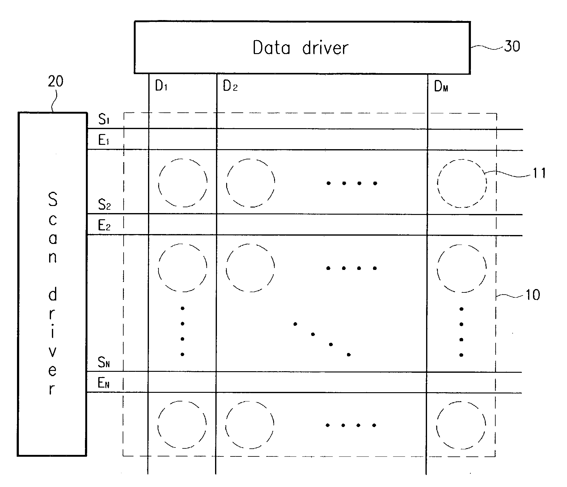
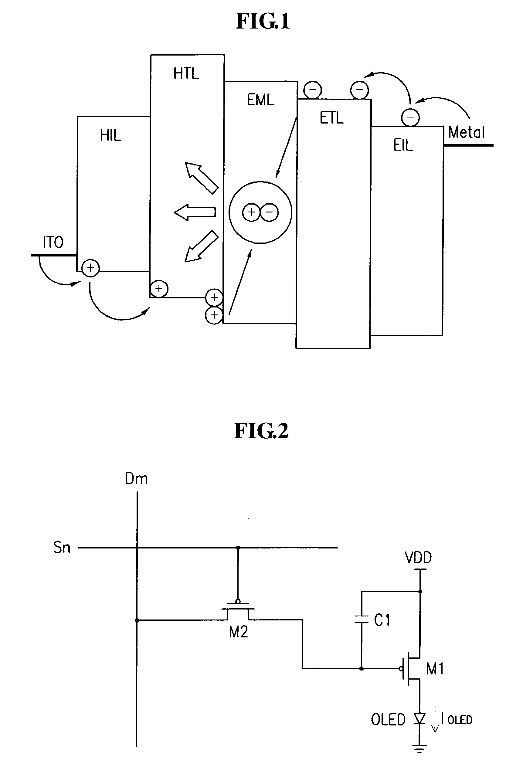
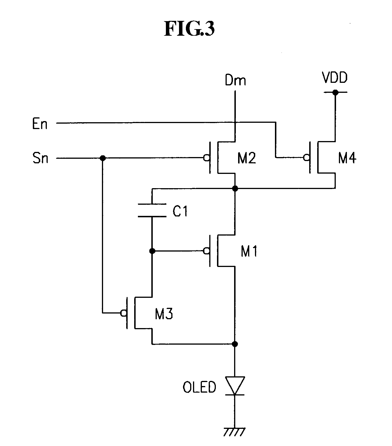
[0033] To clearly describe the various exemplary embodiments of the present invention, portions that are not related to the description are omitted in the drawings. Also, in the following description, similar features of the various exemplary embodiments have identical reference numerals. Further, it should be understood that in the following description, coupling of a first portion to a second portion includes direct coupling of the first portion to the second portion, and coupling of the first portion to the second portion through a third portion provided between the first and second portions. Also, a reference numeral of a s...


PUM


Abstract

A driving transistor for outputting a current for driving an organic electroluminescent (EL) element is formed on a pixel circuit of an organic EL display. A first capacitor is coupled between a power supply voltage and a gate of the driving transistor, and a second capacitor is coupled between the gate and a scan line. First a voltage matched with a data current is stored in the first capacitor in response to a select signal from the scan line. The voltage of the first capacitor is changed by variation of the select signal's voltage level. A driving current is output from the transistor because of the changed voltage of the first capacitor, and the organic EL element emits light as a result of the driving current.

Description

[0001] This application claims priority to and the benefit of Korean Patent Application 2002-32676 filed on Jun. 11, 2002 and Korean Patent Application 2003-17838 filed on Mar. 21, 2003 in the Korean Intellectual Property Office, the content of which are incorporated herein in their entirety by reference.[0002] 1. Field of the Invention[0003] The present invention relates to an organic electroluminescence (EL) light emitting display, a light emitting display panel, and a driving method thereof[0004] 2. Description of the Related Art[0005] An organic EL display is a display that emits light by electrical excitation of fluorescent organic compounds and an image is displayed by driving each of M.times.N organic luminescent cells with voltage or current.[0006] This organic cell includes an anode, an organic thin film and, a cathode layer. The anode may be formed, for example, of indium tin oxide (ITO) and the cathode may be formed, for example, of a metal. The organic thin film is forme...

Claims


Application Information

Patent Timeline
Patent Type & Authority Applications(United States)
IPC IPC(8): H01L51/50G09G3/20G09G3/30G09G3/32
CPCG09G3/325G09G2300/0809G09G2300/0852G09G2300/0861G09G2320/043G09G2310/0262G09G2310/06G09G2320/0223G09G2320/0233G09G2310/0256
Inventor KWON, OH-KYONG
Owner SAMSUNG DISPLAY CO LTD
Why Eureka
Try Eureka