Programmable logic device latch circuits

a latch circuit and logic device technology, applied in the field of latch circuits, can solve problems such as limit performan

Inactive Publication Date: 2006-08-08
ALTERA CORP
View PDF6 Cites 88 Cited by
  • Summary
  • Abstract
  • Description
  • Claims
  • Application Information

AI Technical Summary

Benefits of technology

[0012]In accordance with the present invention, latch circuitry is provided for integrated circuits such as programmable logic device integrated circuits. The latch circuitry may be used to implement a zero-delay latch in which latching functions are provided without incurring significant delay penalties.

Problems solved by technology

While this regularity is beneficial for ease of circuit design, it tends to limit performance in certain situations.

Method used


Image

  • Programmable logic device latch circuits
  • Programmable logic device latch circuits
  • Programmable logic device latch circuits

Examples


Embodiment Construction

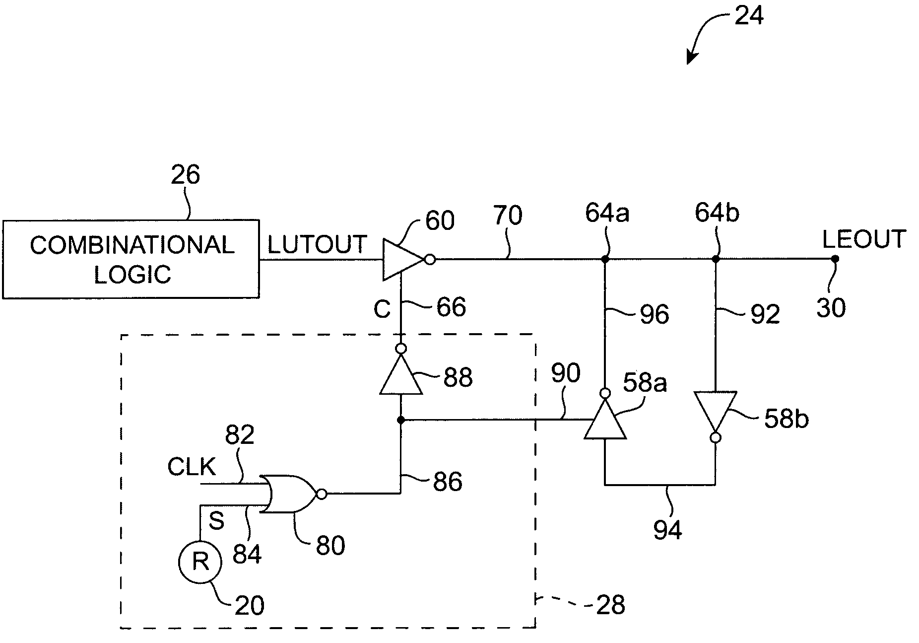
[0039]The present invention relates to latch circuits that may be used to implement latch-based logic circuit designs. The invention also relates to programmable logic regions and programmable logic device integrated circuits that use such latch circuits.

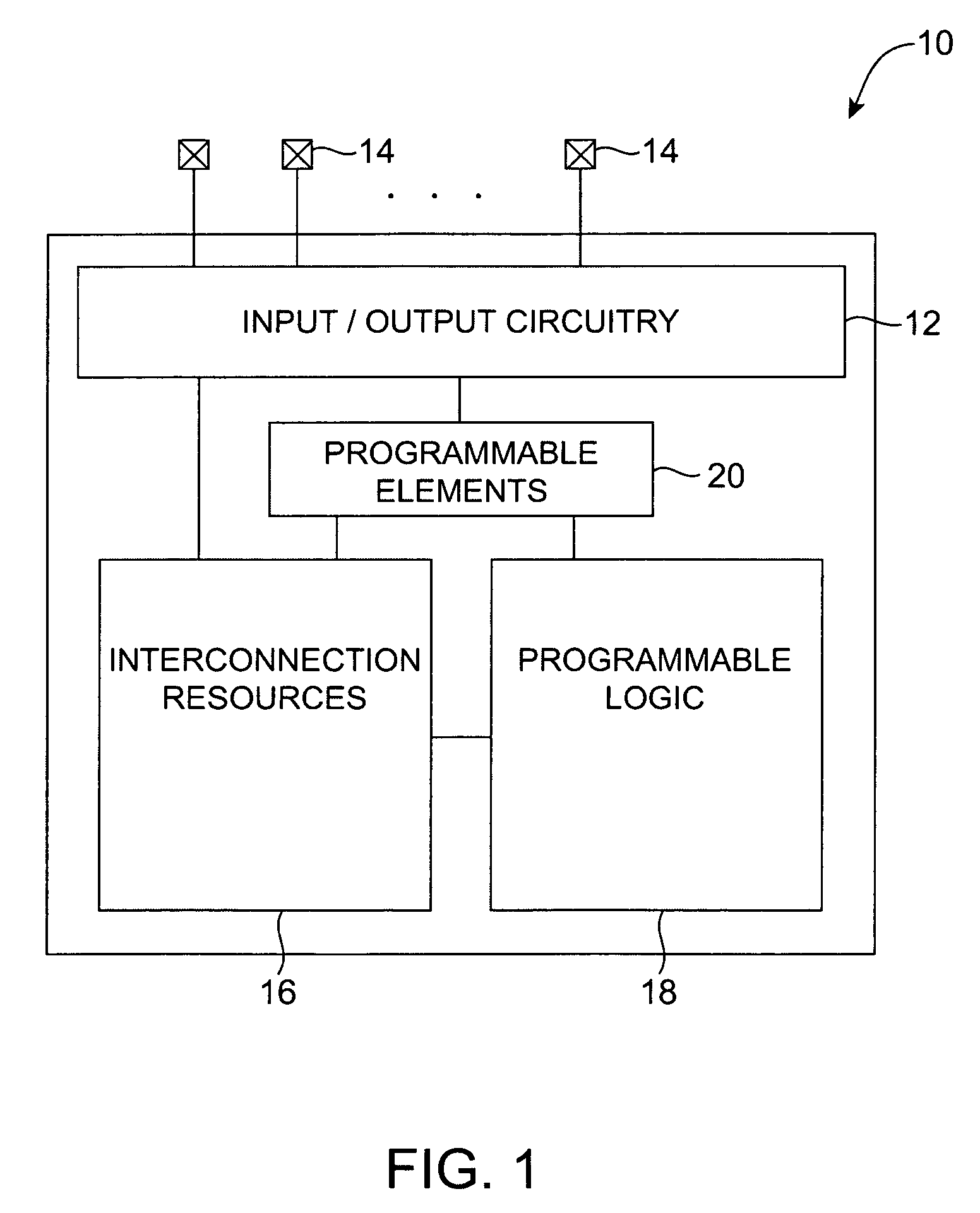
[0040]An illustrative programmable logic device 10 in accordance with the present invention is shown in FIG. 1.

[0041]Programmable logic device 10 may have input / output circuitry 12 for driving signals off of device 10 and for receiving signals from other devices via input / output pins 14. Interconnection resources 16 such as global and local vertical and horizontal conductive lines and busses may be used to route signals on device 10. Programmable logic 18 may include combinational and sequential logic circuitry. The programmable logic 18 may be configured to perform a custom logic function.

[0042]Programmable logic device 10 may be based on any suitable programmable technology. With one suitable approach, configuration data (also cal...


PUM


Abstract

Latch circuitry is provided for programmable logic regions on integrated circuits such as programmable logic device integrated circuits. A programmable logic device may have programmable logic regions based on programmable combinational logic circuits. Latch circuitry in a logic region may be provided between an output of a programmable combinational logic circuit in the logic region and an output of the logic region. When the latch circuitry is enabled, the latch circuitry performs the functions of a level-sensitive latch. When the latch circuitry is disabled, the latch circuitry acts as a passive data path. The passive data path may include only a single driver so that the latch circuitry adds essentially zero additional delay to the data produced by the combinational logic.

Description

BACKGROUND OF THE INVENTION[0001]This invention relates to programmable logic device integrated circuits, and more particularly, to latch circuits for programmable logic devices.[0002]Integrated circuits typically contain combinational logic and sequential logic. Combinational logic does not include storage elements. The output of a given combinational logic circuit is therefore determined solely by its present inputs. Sequential logic circuits contain storage elements that reflect their past behavior. As a result, the output of a sequential circuit is determined by both its present inputs and by the data stored in its storage elements.[0003]Commonly-used sequential circuit storage elements include level-sensitive latches and flip-flops.[0004]In a level-sensitive latch, the latch output is controlled by the level of a clock (enable) input. When the clock is high, the latch output tracks the value of the input. When the clock transitions from high to low, the output state of the latc...

Claims


Application Information

Patent Timeline
Patent Type & Authority Patents(United States)
IPC IPC(8): H03K19/173G06F7/38
CPCH03K19/17792H03K19/17728
Inventor LEWIS, DAVID
Owner ALTERA CORP
Why Eureka
Try Eureka