
Anti-vibration platform for semiconductor equipment

a technology of anti-vibration platform and semiconductor equipment, which is applied in the direction of couplings, rod connections, machine supports, etc., can solve the problems of not fully considering the problem of vibration isolation, providing only very limited protection to the main structure, and developing high-rigidity structures. , to achieve the effect of convenient and rapid transportation and erection, reducing the construction cost, and being safer and more secure for us

Inactive Publication Date: 2006-08-29
TSAI HONG I
View PDF7 Cites 18 Cited by
  • Summary
  • Abstract
  • Description
  • Claims
  • Application Information

AI Technical Summary

Benefits of technology

"The present invention provides an anti-vibration platform for semiconductor equipment that is convenient, safe, durable, and vibration-resistant. The platform is constructed by connecting various components in a secure and easy manner. The components include a ball coupling with threaded holes for connecting to rigid connecting bars and vertical supports. The platform can be easily transported, erected, and repaired, and it is safer and more secure for use. To prevent the components from loosening or separating, elastomeric material is applied to the bottom of the platform for better stability and security."

Problems solved by technology

The conventional high-rigidity structures developed in the early stage did not thoroughly consider the problem of vibration isolation.
However, the current construction design involving vibration isolation, vibration protection or vibration absorption only relates on elastic members attached to the basis of the main structure.
When the platform or the whole structure is subject to vibration, the vibration-isolating means thereof are vibrated at the same time and therefore provide only very limited protection to the main structure.

Method used


Image

  • Anti-vibration platform for semiconductor equipment
  • Anti-vibration platform for semiconductor equipment
  • Anti-vibration platform for semiconductor equipment

Examples


Embodiment Construction

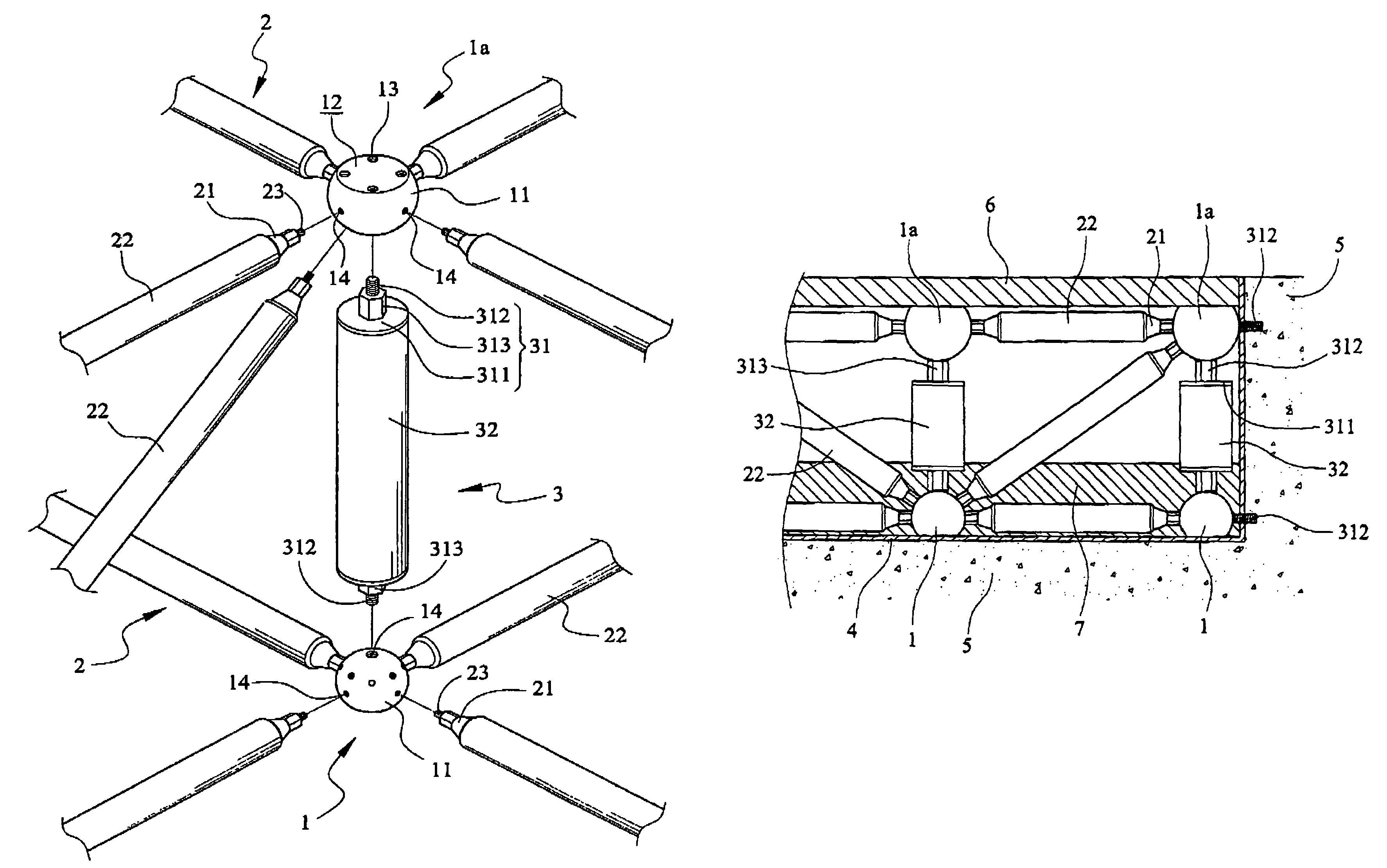
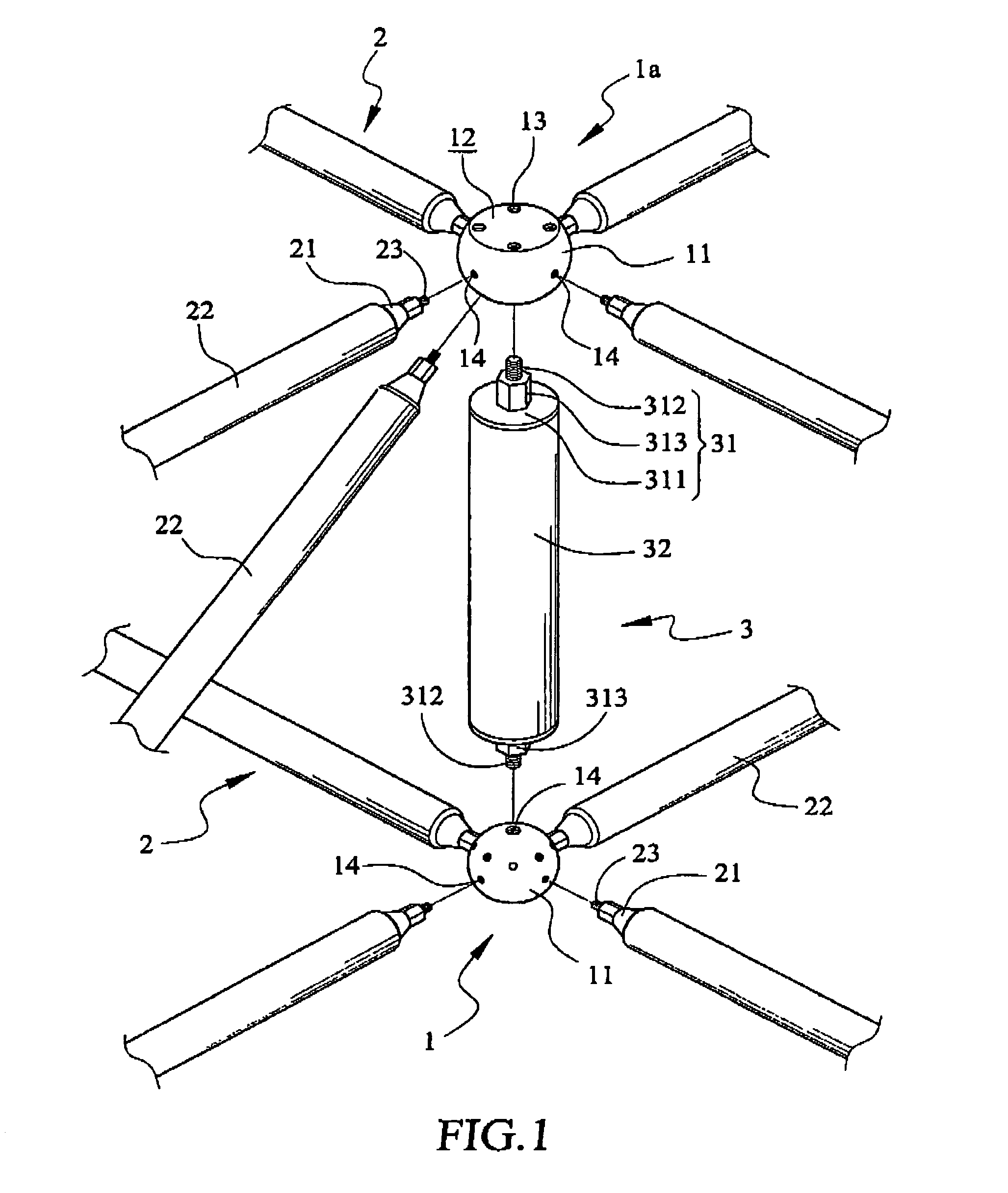
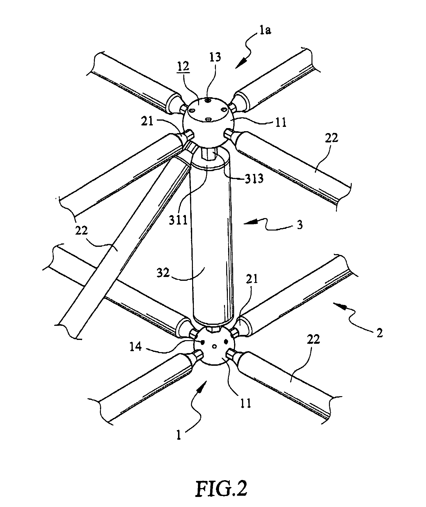
[0018]Please refer to FIGS. 1 and 2 that are fragmentary exploded and assembled perspective views, respectively, of an anti-vibration platform for supporting a semiconductor equipment thereon in accordance with a preferred embodiment of the present invention. As shown, the anti-vibration platform for semiconductor equipment according to the present invention is constructed from a plurality of ball couplings 1 and 1a, a plurality of rigid connecting bars 2, and a plurality of vertical supports 3.

[0019]Each of the ball couplings 1, 1a includes a spherical body 11 having a plurality of internally threaded holes 14 provided at predetermined points on a spherical outer surface thereof.

[0020]The ball coupling 1a is for use at a top of the constructed anti-vibration platform and has a spherical body 11 with a truncated top 12, on which at least one internally threaded hole 13 is provided.

[0021]Each of the rigid connecting bars 2 includes a barred body 22 having a predetermined length, and ...


PUM


Abstract

An anti-vibration platform for supporting a semiconductor equipment is constructed from a plurality of top and bottom ball couplings having threaded holes provided thereon, a plurality of rigid connecting bars separately horizontally or diagonally connected at two externally threaded free ends to two of the ball couplings, and a plurality of vertical supports separately connected at two externally threaded free ends to two vertically corresponding ball couplings. Steel plates are provided at a bottom and four sides of the platform, and threaded bars are provided to extend through the side steel plates to connect the platform to a concrete foundation. Anti-vibration and pressure-resistant elastomeric material is applied to the bottom of the platform to wrap joints of the bottom ball couplings, the connecting bars, and the vertical supports. A flat bed is positioned to a top of the platform by screwing to the top ball couplings.

Description

BACKGROUND OF THE INVENTION[0001]1. Field of the Invention[0002]The present invention relates to an anti-vibration platform, and more particularly to an anti-vibration platform for semiconductor equipment that is constructed by assembling a plurality of ball couplings, connecting bars, and vertical supports to one another, and provided with special anti-vibration measures to be safer and more convenient and durable for use.[0003]2. Description of the Prior Art[0004]Most of the conventional platforms for supporting semiconductor equipment are constructed by welding steel frames together and then provided the welded steel frames with flexible vibration-isolating structures. For example, the vibration-isolating structure disclosed in Taiwan Publication No. 530862 includes horizontal upper and lower base plates, and a column vertically connected to and located between the upper and the lower plates via upper and lower annular cushions. The vertical column is provided around its outer su...

Claims


Application Information

Patent Timeline
Patent Type & Authority Patents(United States)
IPC IPC(8): F16M1/00E04B1/19E04F15/024F16B7/18F16F15/00
CPCE04F15/02458F16B7/185F16F15/00E04B1/1906E04B2001/1927E04B2001/196E04B2001/1984Y10T403/34Y10T403/341E04B2001/199E04F2015/02055
Inventor TSAI, HONG-I
Owner TSAI HONG I
Learn More