

Semiconductor memory cell and semiconductor memory device
a memory cell and semiconductor technology, applied in the field of semiconductor memory devices, can solve the problems of inability to control neither the position of grain boundaries containing crystals, nor the reliability, and achieve the effects of less fluctuation in characteristic, high field effect mobility, and controllable crystallinity of channel regions of tfts and semiconductor memory cells
- Summary
- Abstract
- Description
- Claims
- Application Information
AI Technical Summary
Benefits of technology
Problems solved by technology
Method used
Image

Examples
embodiment mode 1
[0072]A circuit structure and operation method of a non-volatile memory will be described as an embodiment mode of a semiconductor memory device of the present invention.
[0073]Features of the present invention are in the structure of a semiconductor memory cell and its semiconductor active layer and in the structure and semiconductor active layers of TFTs that constitute peripheral circuits. For the circuit structure and operation method of a memory cell, known techniques are used. This embodiment mode gives a brief description on the circuit structure and operation method of a NOR flash memory as a typical non-volatile memory.
[0074]FIG. 7 is a block circuit diagram of a NOR flash memory having a storage capacity of m×n bits: The NOR flash memory shown in FIG. 7 is composed of a memory cell array 701 and peripheral circuits including an X address decoder 703, a Y address decoder 702, a Y selector 704, and a writing / reading circuit 705. The memory cell array 701 has plural memory cel...
embodiment mode 2
[0083]A method of forming a crystalline semiconductor film in the present invention will be described. The description is given with reference to FIGS. 3A to 6B. In perspective views of FIGS. 3A and 3B, a first insulating film 302 and second insulating films 303 to 306 form stripe pattern concave portions on a substrate 301. Although FIGS. 3A and 3B show three linear concave portions, the number of linear concave portions is not limited thereto.
[0084]The substrate employed is a commercially-available non-alkaline glass substrate, quartz substrate, sapphire substrate, or single crystal or polycrystal semiconductor substrate with its surface covered with an insulating film. Alternatively, a metal substrate with its surface covered with an insulating film may be employed.
[0085]To form the stripe pattern concave portions with a sub-micron level design rule, it is necessary to reduce unevenness on the substrate surface and warpage or contortion of the substrate down to the depth of focus...
embodiment mode 3
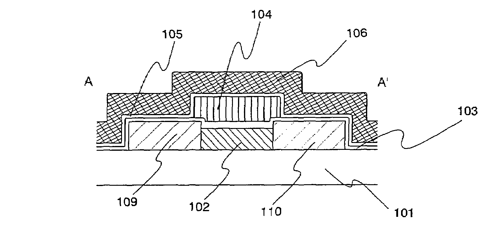
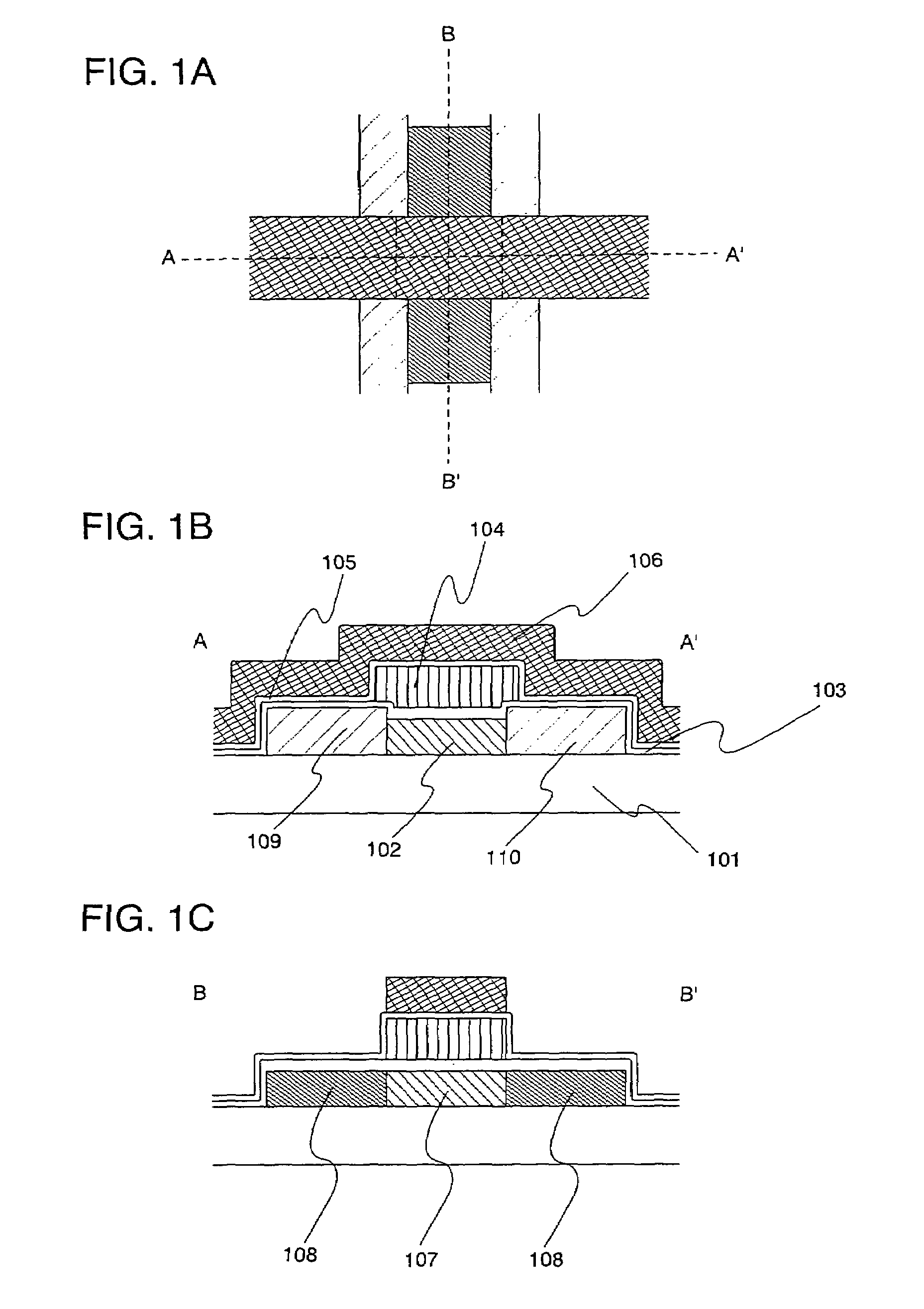
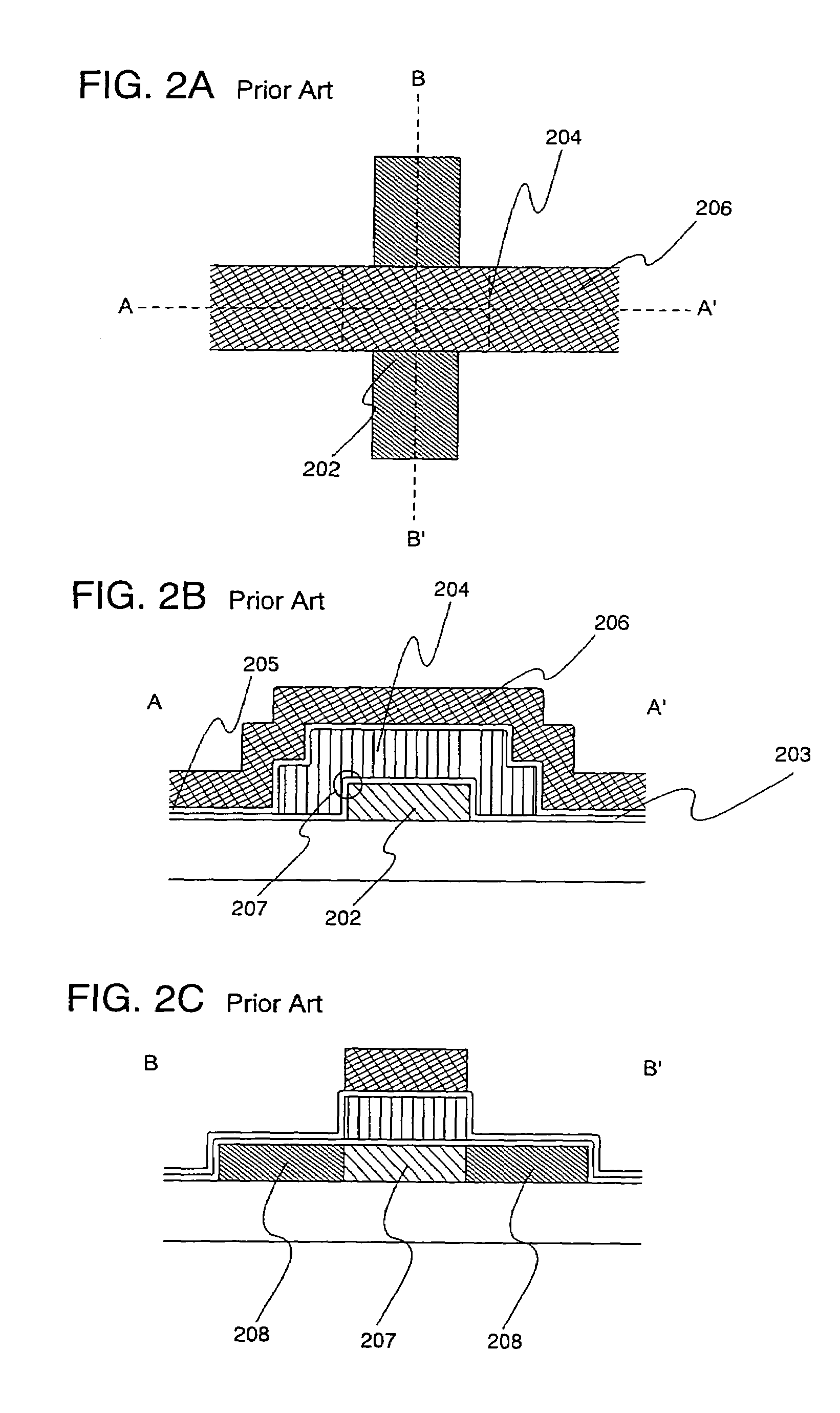
[0110]Referring to the drawings, a description is given on a mode of manufacturing a semiconductor memory cell and a TFT whose channel formation regions are placed in filling regions of a crystalline silicon film on a base insulating film that has concave portions. The filling regions are portions of the crystalline silicon film that fill the concave portions. In each of the drawings for this embodiment mode, (1) is a top view whereas (2) to (5) are sectional views of several portions in the top view.
[0111]In the mode shown in this embodiment mode, a memory cell array and peripheral circuits are manufactured simultaneously. On the right hand of the drawings is a part of a NOR memory cell array in which semiconductor memory cells are arranged to form a matrix pattern. Shown on the left hand of the drawings as a representative of the peripheral circuits is an inverter composed of an n-channel TFT and a p-channel TFT.
[0112]FIGS. 8A to 8E show a mode in which a first insulating film 802...
PUM
 Abstract
Description
Claims
Application Information