Electron-emitting device, electron source, image display apparatus and method of fabricating electron-emitting device

a technology of electron emission and image display, which is applied in the manufacture of electrode systems, electric discharge tubes/lamps, and discharge tubes luminescnet screens, etc., can solve the problem of occasional generation of intensive stress, and achieve the effect of less fluctuation of electron emission amoun

Inactive Publication Date: 2007-11-08
CANON KK
View PDF15 Cites 13 Cited by
  • Summary
  • Abstract
  • Description
  • Claims
  • Application Information

AI Technical Summary

Benefits of technology

[0011]Therefore, an object of the present invention is to provide an electron-emitting device with less fluctuation in electron emission amount, with an electron emission layer restrained to get delaminated from a substrate and a member (for example, cathode electrode) in contact with the electron emission layer and with less fluctuation in electron-emitting properties and a method of fabricating the electron-emitting device.
[0016]According to the present invention, there can be provided an electron-emitting device which is prevented from being delaminated from a substrate and does not require any resistance layer for limiting current to be provided except a cathode electrode and presents less fluctuation in electron emission amount and a method of fabricating the electron-emitting device.

Problems solved by technology

However, depending on material and thickness of respective members configuring the electron-emitting device, intensive stress is occasionally generated.

Method used


Image

  • Electron-emitting device, electron source, image display apparatus and method of fabricating electron-emitting device
  • Electron-emitting device, electron source, image display apparatus and method of fabricating electron-emitting device
  • Electron-emitting device, electron source, image display apparatus and method of fabricating electron-emitting device

Examples


example 1

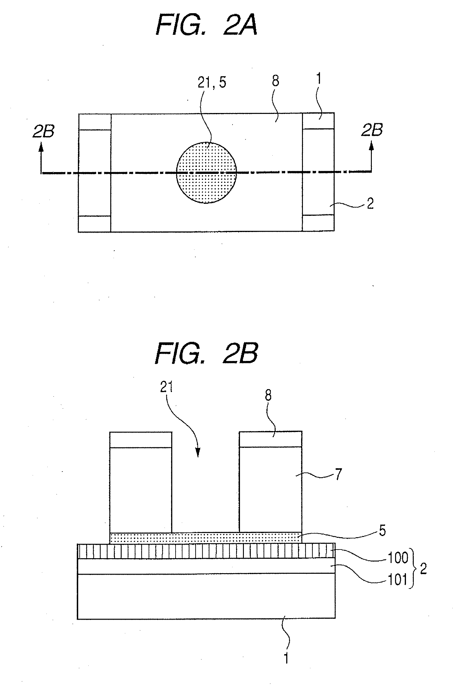
[0142]An electron-emitting device illustrated in FIGS. 2A and 2B are produced according to the process illustrated in FIGS. 6A to 6H.

[0143](Process 1)

[0144]A silica substrate is used as the substrate 1, which is cleaned sufficiently. Thereafter, in order to form a great number of columnar regions 3 on the substrate 1, TiN film with a thickness of 100 nm is formed with the sputtering method under condition 1 to be described below. As for atmosphere gas for the condition 1 to be described below, gas mixed in proportion of Ar gas to N2 gas being 9:1 is used.

[0145](Condition 1)[0146]Rf power supply: 13.56 MHz[0147]Rf output: 8 W / cm2 [0148]Atmosphere gas pressure: 1.2 Pa[0149]Target: Ti

[0150]The formed TiN film was configured by a great number of columnar regions 3 as illustrated in FIG. 6A. The average diameter W of the columnar regions 3 was 30 nm and the resistivity ρ3 thereof was 10−4 Ω·cm. The surface of the formed TiN film undergoes image taking at a magnification of 0.2 million ti...

example 2

[0186]In the present example, electron-emitting device illustrated in FIGS. 2A and 2B was produced according to the process illustrated in FIGS. 8A to 8H. Here, the electron-emitting device of the example 2 is an electron-emitting device configured by an electron emission layer 5 arranged only inside the opening 21 unlike the example 1.

[0187](Process 1)

[0188]As in the process 1 of the example 1, there formed were columnar regions 3 including a great number of TiN on the substrate 1 (FIG. 8A). The average diameter of the columnar regions 3 was 30 nm. The resistivity ρ3 thereof was 10−4 Ω·cm.

[0189](Process 2)

[0190]Next, the substrate 1 was put in an ashing device of the ozone atmosphere and underwent ozone ashing. Then, second regions 4 mainly comprising an oxide of Ti were formed between a plurality of the adjacent TiN columnar regions 3 (sides of the columnar regions 3). In addition, at the same time, an oxide layer 12 was formed over the surface of the columnar regions 3.

[0191]As a...

example 3

[0211]With the electron-emitting device produced in the above described example 2, an electron-emitting device 57 illustrated in FIG. 5 was produced.

[0212]One hundred each of the electron-emitting devices illustrated in the example 2 were arranged in the X direction and in the Y direction to shape a matrix. As to wiring, the X direction wiring 42 (Dx1 to Dxm) was connected to the electroconductive layer 2 and the Y direction wiring 43 (Dy1 to Dyn) was connected to the gate electrode 8 as illustrated in FIG. 5. A phosphor layer 54 and metal back 55 being an anode electrode were arranged above the respective electron-emitting devices 44. FIG. 5 illustrates an example where a single opening 21 is formed in a single electron-emitting device 44. However, the number of the openings will not be limited to one, but a plurality of openings may be provided.

[0213]In order to seal the envelope 57, the rear plate 1 and the face plate 56 were sealed to sandwich the support frame 52 in between wit...


PUM


Abstract

There are provided a stable electron-emitting device with less fluctuation in electron-emitting properties and a method of fabricating the electron-emitting device. The electron-emitting device has a substrate; a plurality of columnar first regions respectively orientated substantially perpendicular to the surface of the substrate; a second region provided between the respective first regions higher than the first regions in resistance; and an electron emission layer covering the columnar first regions and the second region.

Description

BACKGROUND OF THE INVENTION[0001]1. Field of the Invention[0002]The present invention relates to an electron-emitting device, an electron source including the electron-emitting devices and an image display apparatus including the electron source.[0003]2. Description of the Related Art[0004]The electron-emitting device includes an electron-emitting device of a field-emission type (hereinafter to be referred to as “FE type”) and an electron-emitting device of a surface conduction type.[0005]As an electron-emitting device of the FE type, an electron-emitting device having an electron beam with less spread is exemplified by an electron-emitting device comprising a gate electrode provided with openings (so-called “gate halls”) on flat electron-emitting film as in Japanese Patent Application Laid-Open No. 2004-071536, Japanese Patent Application Laid-Open No. H08-055564 and Japanese Patent Application Laid-Open No. 2005-26209. In the electron-emitting device including such a flat electron...

Claims


Application Information

Patent Timeline
Patent Type & Authority Applications(United States)
IPC IPC(8): H01J1/00H01J19/06H01J1/62
CPCH01J1/304H01J31/127H01J9/025
Inventor MURAKAMI, SHUNSUKE
Owner CANON KK
Why Eureka
Try Eureka