

Electron-emitting device, electron source, image display apparatus and method of fabricating electron-emitting device
a technology of electron emission and image display, which is applied in the manufacture of electrode systems, electric discharge tubes/lamps, and discharge tubes luminescnet screens, etc., can solve the problem of occasional generation of intensive stress, and achieve the effect of less fluctuation of electron emission amoun
- Summary
- Abstract
- Description
- Claims
- Application Information
AI Technical Summary
Benefits of technology
Problems solved by technology
Method used
Image

Examples
example 3
[0117]With the electron-emitting device produced in the above described example 2, an electron-emitting device 57 illustrated in FIG. 5 was produced.
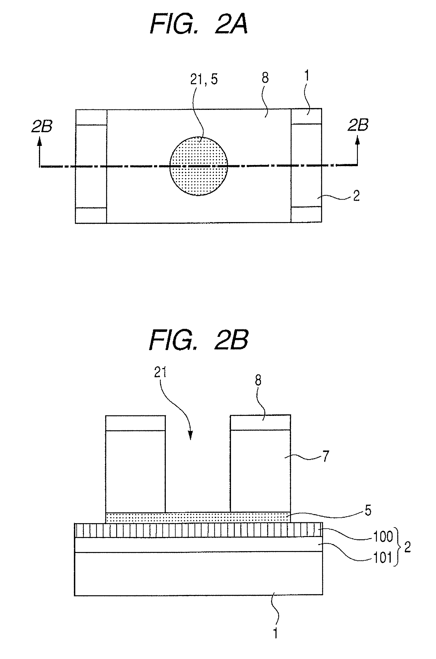
[0118]One hundred each of the electron-emitting devices illustrated in the example 2 were arranged in the X direction and in the Y direction to shape a matrix. As to wiring, the X direction wiring 42 (Dx1 to Dxm) was connected to the electroconductive layer 2 and the Y direction wiring 43 (Dy1 to Dyn) was connected to the gate electrode 8 as illustrated in FIG. 5. A phosphor layer 54 and metal back 55 being an anode electrode were arranged above the respective electron-emitting devices 44. FIG. 5 illustrates an example where a single opening 21 is formed in a single electron-emitting device 44. However, the number of the openings will not be limited to one, but a plurality of openings may be provided. processes (a) to (d), the insulating layer 7 is deposited over the electron emission layer 5 (FIG. 3F).
[0119]The insulating layer 7 may b...
example 1
[0146]An electron-emitting device illustrated in FIGS. 2A and 2B are produced according to the process illustrated in FIGS. 6A to 6H.
[0147](Process 1)
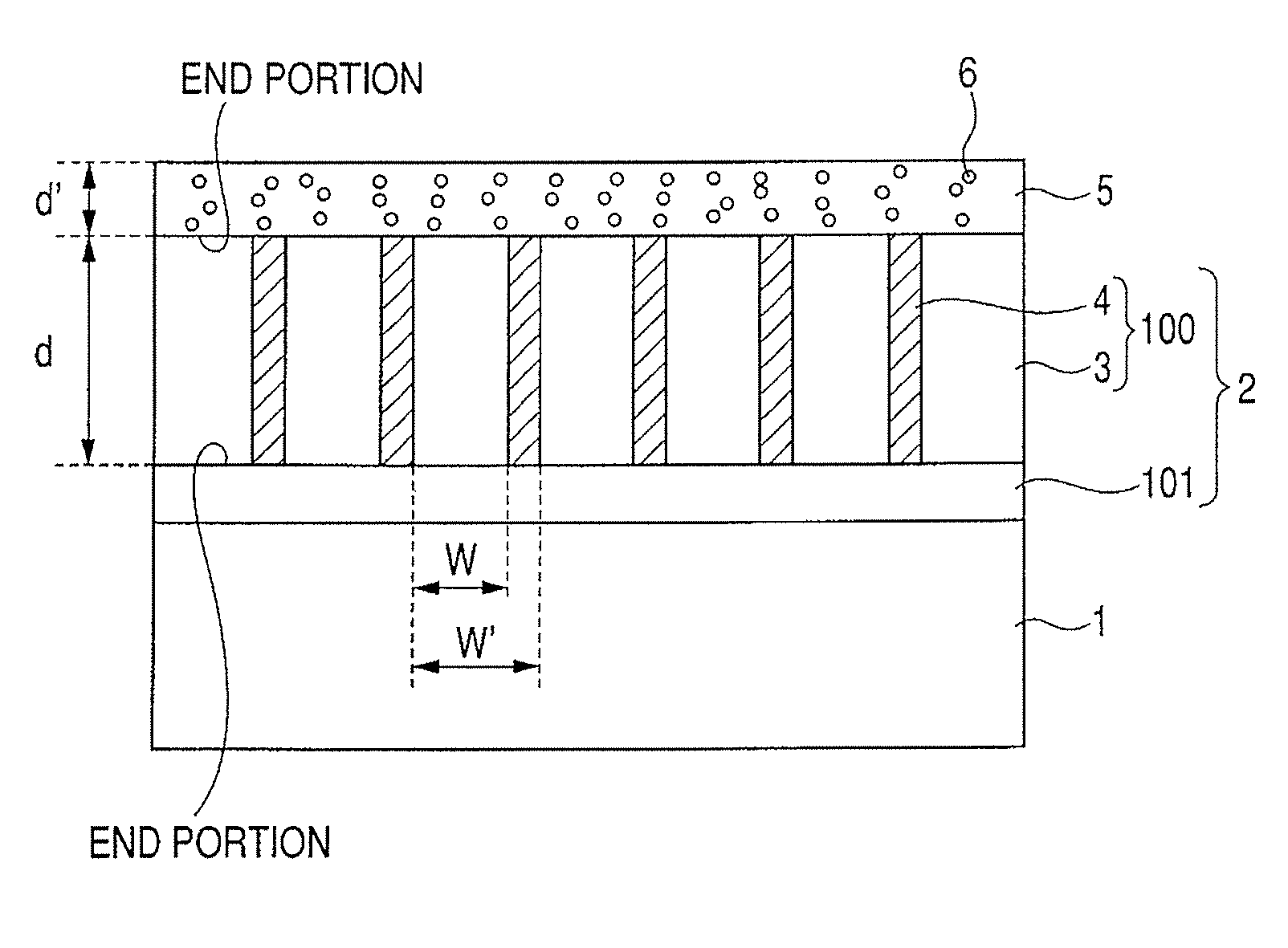
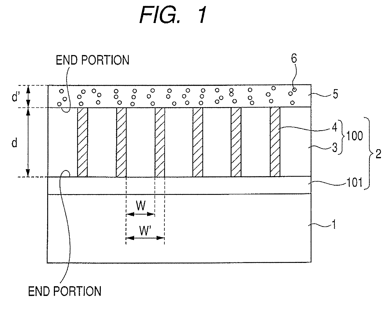
[0148]A silica substrate is used as the substrate 1, which is cleaned sufficiently. Thereafter, in order to form a great number of columnar regions 3 on the substrate 1, TiN film with a thickness of 100 nm is formed with the sputtering method under condition 1 to be described below. As for atmosphere gas for the condition 1 to be described below, gas mixed in proportion of Ar gas to N2 gas being 9:1 is used.
[0149](Condition 1)[0150]Rf power supply: 13.56 MHz[0151]Rf output: 8 W / cm2 [0152]Atmosphere gas pressure: 1.2 Pa[0153]Target: Ti
[0154]The formed TiN film was configured by a great number of columnar regions 3 as illustrated in FIG. 6A. The average diameter W of the columnar regions 3 was 30 nm and the resistivity ρ3 thereof was 10−4 Ω·cm. The surface of the formed TiN film undergoes image taking at a magnification of 0.2 million ti...
example 2
[0190]In the present example, electron-emitting device illustrated in FIGS. 2A and 2B was produced according to the process illustrated in FIGS. 8A to 8H. Here, the electron-emitting device of the example 2 is an electron-emitting device configured by an electron emission layer 5 arranged only inside the opening 21 unlike the example 1.
[0191](Process 1)
[0192]As in the process 1 of the example 1, there formed were columnar regions 3 including a great number of TiN on the substrate 1 (FIG. 8A). The average diameter of the columnar regions 3 was 30 nm. The resistivity ρ3 thereof was 10−4 Ω·cm.
[0193](Process 2)
[0194]Next, the substrate 1 was put in an ashing device of the ozone atmosphere and underwent ozone ashing. Then, second regions 4 mainly comprising an oxide of Ti were formed between a plurality of the adjacent TiN columnar regions 3 (sides of the columnar regions 3). In addition, at the same time, an oxide layer 12 was formed over the surface of the columnar regions 3.
[0195]As a...
PUM
 Abstract
Description
Claims
Application Information