Solid electrolytic capacitor

Active Publication Date: 2007-02-08
MURATA MFG CO LTD
View PDF11 Cites 11 Cited by
  • Summary
  • Abstract
  • Description
  • Claims
  • Application Information

AI Technical Summary

Benefits of technology

[0013] Further, the present inventors have found that imparting the cut surface formed by the elongation of the valve-acting metal layer without having pores of the chamfered anode substrate when dragged by a cutting blade with a structure having grooves obliquely or parallel to the direction of the short axis with a structure having grooves obliquely or parallel to the direction of the short axis helps the absorption of solution to the surface of the valve-acting metal without ability of retaining the solution, thereby having an effect on facilitating forming the electrically-conducting polymer film more uniformly.
[0014] Therefore, the present inventors have produced a solid electrolytic capacitor using a cut foil o

Problems solved by technology

If the polymerization conditions of the electrically conducting polymer in the cathode portion of the capacitor element are not precisely controlled, the thickness of the electrically conducting polymer becomes uneven and the electrically conducting polymer comes to have a thin portion, in which direct contact of the paste or the like with the dielectric oxide film layer readily occurs, giving rise to increase in the leakage current.
Furthermore, since the number of capacitor elements which can be stacked in a solid electrolytic capacitor chip having a predetermined size is limited by the thickness of the element, the capacitance of the solid electrolytic capacitor chip cannot be increased.
Specifically, in a capacitor elemen

Method used


Image

  • Solid electrolytic capacitor
  • Solid electrolytic capacitor
  • Solid electrolytic capacitor

Examples


Example

Example 1

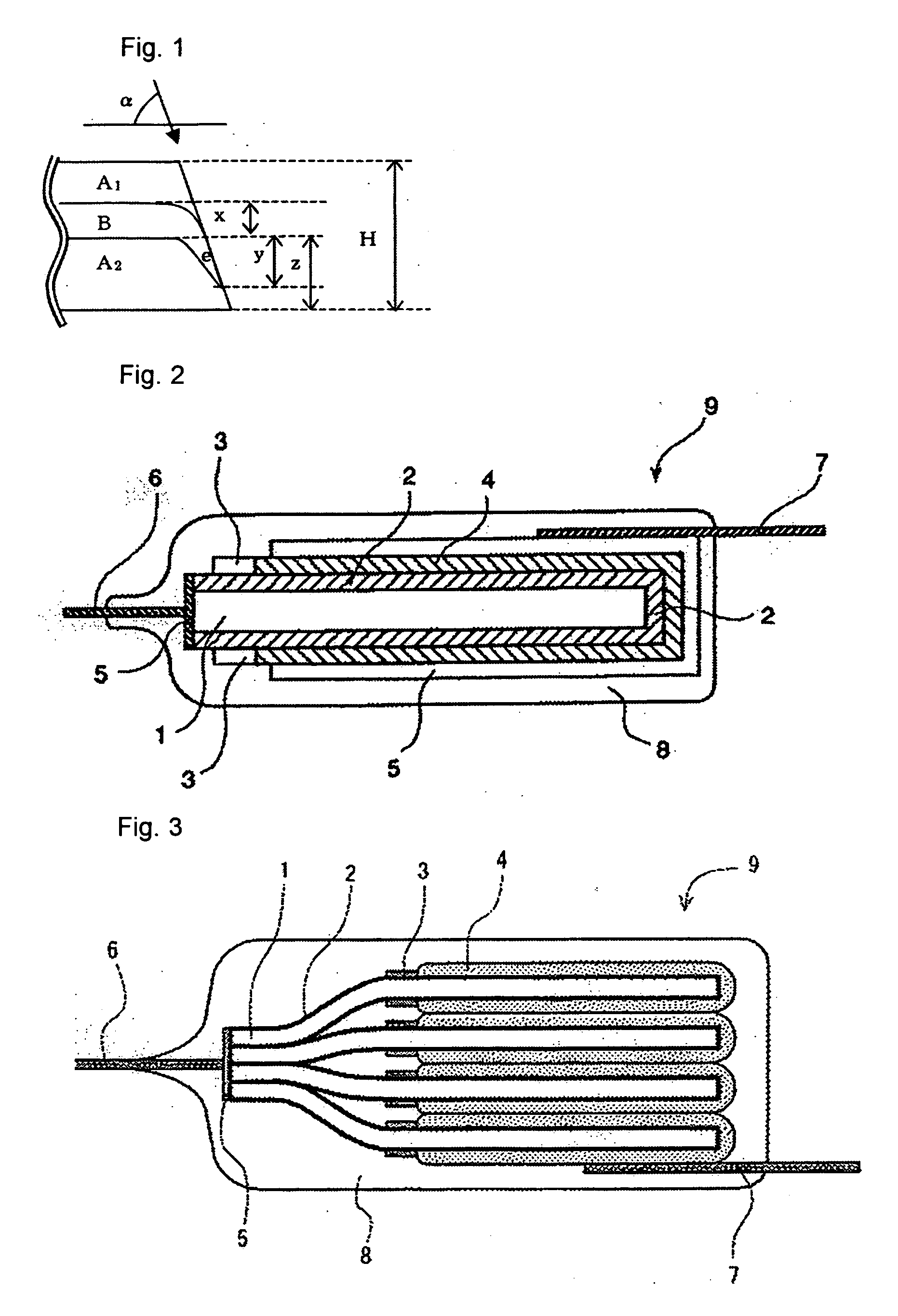
[0172] A chemically formed aluminum foil in which x and y / z in FIG. 1 are respectively 30 μm and 0.3, a supplementary angle of cutting angle α (see FIG. 1) is 110°, the thickness as a whole (H) is 110 μm was used. Its enlarged cross-sectional photograph is shown in FIG. 4. Also, an enlarged photograph of the cut surface is shown in FIG. 10. The aluminum foil was cut into a size of 3 mm (short axis direction) ×10 mm (long axis direction), and a polyimide solution was circumferentially coated on both surfaces in a width of 1 mm to divide the surface into a 4-mm portion and a 5-mm portion in the long axis direction and then dried to provide a masking. A voltage of 4 V was applied to the 3 mm×4 mm portion of this chemically formed foil in a 10 mass % aqueous ammonium adipate solution to chemically form the cut end part and thereby produce a dielectric oxide film. Thereafter, this 3 mm×4 mm portion of the aluminum foil was dipped in a 2.0 mol / L isopropyl alcohol (IPA) solution ...

Example

Example 2

[0176] A chemically formed aluminum foil in which x and y / z in FIG. 1 are respectively 30 μm and 0.5, a supplementary angle of cutting angle α (see FIG. 1) is 110°, the thickness as a whole (H) is 110 μm was used. Its enlarged cross-sectional photograph is shown in FIG. 5. Except using this chemically formed aluminum foil, a solid electrolyte was formed in the same manner as in Example 1.

[0177] The film thickness at a corner part (the cut section at an inner angle of 110° between the edges) measured in the same manner as in Example 1 was 19 μm.

[0178] Thereafter, the re-chemical formation, the coating of a carbon paste and a silver paste, the stacking, the connection of a cathode lead terminal, the encapsulation with an epoxy resin, and the aging operation were performed in the same manner as in Example 1, and 30 units in total of capacitors were completed. The properties of the obtained laminated capacitor devices were evaluated in the same manner as in Example 1 and the...

Example

Example 3

[0179] A chemically formed aluminum foil in which x and y / z in FIG. 1 are respectively 30gm and 0.8, a supplementary angle of cutting angle α (see FIG. 1) is 1100, the thickness as a whole (H) is 110 μm was used. Its enlarged cross-sectional photograph is shown in FIG. 6. Except using this chemically formed aluminum foil, a solid electrolyte was formed in the same manner as in Example 1.

[0180] The film thickness at a corner part (the cut section at an inner angle of 110° between the edges) measured in the same manner as in Example 1 was 17 μm.

[0181] Thereafter, the re-chemical formation, the coating of a carbon paste and a silver paste, the stacking, the connection of a cathode lead terminal, the encapsulation with an epoxy resin, and the aging operation were performed in the same manner as in Example 1, and 30 units in total of capacitors were completed. The properties of the obtained laminated capacitor devices were evaluated in the same manner as in Example 1 and the ...


PUM

PropertyMeasurementUnit
Angleaaaaaaaaaa
Angleaaaaaaaaaa
Angleaaaaaaaaaa

Abstract

The present invention relates to an anode substrate for a solid electrolytic capacitor which is produced by cutting obliquely a metal substrate comprising a valve-acting metal layer having fine pores and a valve-acting metal layer without fine pores, and having a cut surface which is formed by elongation of the valve-acting metal layer without fine pores dragged by a cutting blade; particularly to an anode substrate for a solid electrolytic capacitor which is produced by cutting obliquely a metal substrate comprising a valve-acting metal layer having fine pores and a valve-acting metal layer without fine pores, and a layer of the elongated valve-acting metal which is generated by that the valve-acting metal layer without fine pores is elongated being dragged along with a cutting blade and covers the edge part of the valve-acting layer having fine pores meets the requirement represented by the following formula:
0≦y/z≦1  [Formula 1]
wherein y represents the thickness of the layer of the elongated valve-acting metal in the direction of the thickness of the substrate and z represents the thickness of the valve-acting layer having fine pores which is in contact with the elongated metal layer in the direction of the thickness of the substrate, respectively; and to a solid electrolytic capacitor comprising the above-mentioned anode substrate, an edge of which is chamfered at least partially.

Description

CROSS REFERENCE TO THE RELATED APPLICATIONS [0001] This is an application filed pursuant to 35 U.S.C. Section 111(a) with claiming the benefit of U.S. Provisional Application Ser. No. 60 / 677,407 filed May 4, 2005 and No. 60 / 677,806 filed May 5, 2005 under the provision of 35 U.S.C. Section 111(b), pursuant to 35 U.S.C. Section 119(e) (1).TECHNICAL FIELD [0002] The present invention relates to a solid electrolytic capacitor using an electrically conducting polymer as the solid electrolyte layer, and a production method thereof. BACKGROUND ART [0003] The basic element of a solid electrolytic capacitor is generally produced, as shown in FIG. 2, by forming a dielectric oxide film layer (2) on an anode substrate (1) comprising a metal foil subjected to an etching treatment to have a large specific surface area, forming a solid semiconductor layer (hereinafter referred to as a “solid electrolyte”) (4) as a counter electrode on the outer side of the dielectric oxide layer, and preferably f...

Claims


Application Information

Patent Timeline
IPC IPC(8): H01G4/255
CPCH01G9/012H01G9/042Y10T29/417H01G9/15H01G9/055
Inventor SAIDA, YOSHIHIROASAI, YOSHIFUMIOOHATA, HIDEKI
Owner MURATA MFG CO LTD
Why Eureka
Try Eureka