Nanostructured light-emitting device

Active Publication Date: 2013-01-17
SAMSUNG ELECTRONICS CO LTD
View PDF9 Cites 12 Cited by
  • Summary
  • Abstract
  • Description
  • Claims
  • Application Information

AI Technical Summary

Benefits of technology

This patent describes a light-emitting device with nanostructures that have a more uniform p-type semiconductor layer. The device includes a first type semiconductor layer, nanostructures with a 3D shape, an active layer, and a second type semiconductor layer. The nanostructures can be divided into groups, and the second type semiconductor layer can be connected to the active layers of adjacent nanostructures. The device can also include a mask layer and nano-holes for growing the nanostructures. The technical effect of this patent is to provide a more uniform p-type semiconductor layer and improved performance of the light-emitting device.

Problems solved by technology

However, as a general matter, many crystal defects exist in nitride-based compound semiconductor crystals.

Method used


Image

  • Nanostructured light-emitting device
  • Nanostructured light-emitting device
  • Nanostructured light-emitting device

Examples


Embodiment Construction

[0037]Reference will now be made in detail to embodiments, examples of which are illustrated in the accompanying drawings, wherein like reference numerals refer to like elements throughout. In this regard, the embodiments may have different forms and should not be construed as being limited to the descriptions set forth herein. Accordingly, the embodiments are merely described below, by referring to the figures, to explain aspects of the present description. In the drawings, the thicknesses of layers and regions may be exaggerated for clarity.

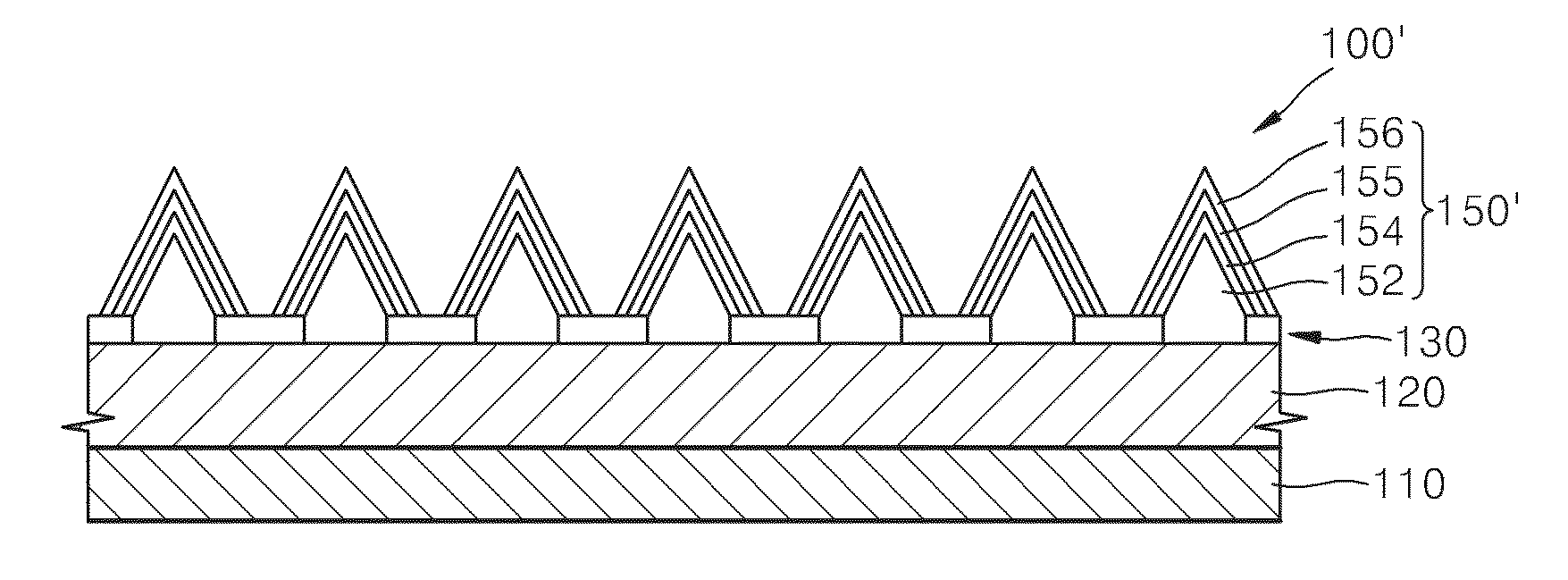
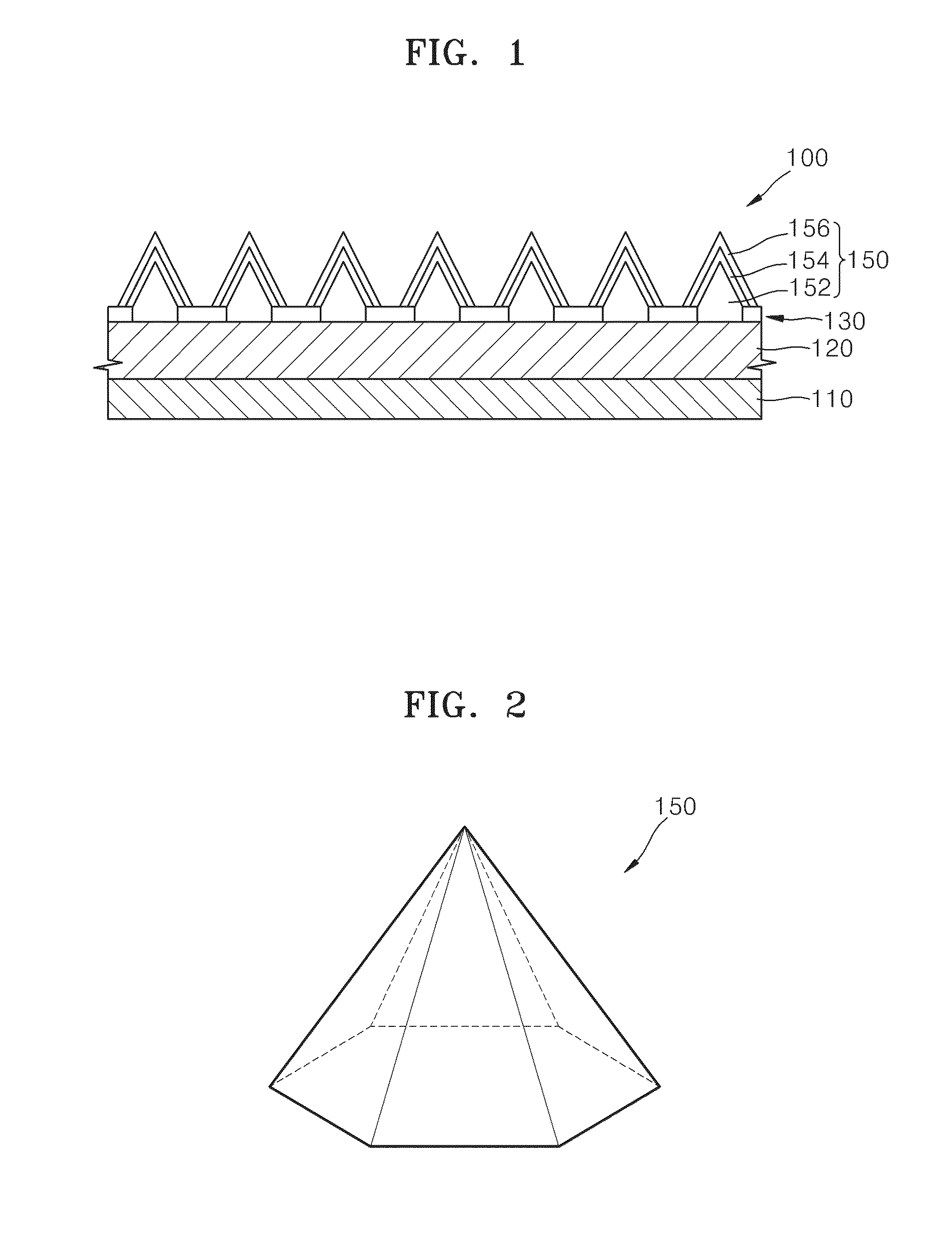
[0038]FIG. 1 is a cross-sectional view of a light-emitting device 100 according to an embodiment and FIG. 2 is a perspective view of a shape of one of a plurality of nanostructures 150 of the light-emitting device 100 illustrated in FIG. 1.

[0039]Referring to FIGS. 1 and 2, the light-emitting device 100 includes a first type semiconductor layer 120 and a plurality of nanostructures 150 formed on the first type semiconductor layer 120. Each of th...


PUM


Abstract

A nanostructured light-emitting device including: a first type semiconductor layer; a plurality of nanostructures each including a first type semiconductor nano-core grown in a three-dimensional (3D) shape on the first type semiconductor layer, an active layer formed to surround a surface of the first type semiconductor nano-core, and a second type semiconductor layer formed to surround a surface of the active layer and including indium (In); and at least one flat structure layer including a flat-active layer and a flat-second type semiconductor layer that are sequentially formed on the first type semiconductor layer parallel to the first type semiconductor layer.

Description

CROSS-REFERENCE TO RELATED APPLICATIONS[0001]This application claims priority from Korean Patent Application No. 10-2011-0068978, filed on Jul. 12, 2011 in the Korean Intellectual Property Office, the disclosure of which is incorporated herein in its entirety by reference.BACKGROUND[0002]1. Field[0003]The present disclosure relates to nanostructured light-emitting devices.[0004]2. Description of the Related Art[0005]Semiconductor light-emitting devices are light sources that have high efficiency and are eco-friendly. Semiconductor light-emitting devices are used in a variety of fields, such as displays, optical communication, vehicles, general illumination, and the like. The range of applications in which semiconductor light-emitting devices are used is increasing, as blue light-emitting devices and ultraviolet (UV)-ray emitting devices using nitride having excellent physical and chemical characteristics have recently emerged. The further emergence of white light or other single-col...

Claims


Application Information

Patent Timeline
IPC IPC(8): H01L33/40B82Y99/00
CPCH01L33/08H01L33/24B82Y20/00B82Y30/00B82Y40/00H01L33/32H01L33/04
Inventor KIM, JOO-SUNGKIM, TAEKYANG, MOON-SEUNG
Owner SAMSUNG ELECTRONICS CO LTD
Why Eureka
Try Eureka