Stacked microelectronic assemblies

a technology of microelectronic assemblies and stacking, which is applied in the direction of electrical apparatus contruction details, semiconductor/solid-state device details, printed circuit non-printed electric components association, etc., can solve the problems of increasing the overall size of the package, affecting the processing and feeding of stacking packages, and affecting the placement of packages

Inactive Publication Date: 2006-12-12
TESSERA INC
View PDF57 Cites 62 Cited by
  • Summary
  • Abstract
  • Description
  • Claims
  • Application Information

AI Technical Summary

Problems solved by technology

However, inaccuracies in folding the substrate can cause parts of the package to lie in positions different from their intended position relative to the mounting terminals.
This effectively increases the overall size of the package.
Moreover, the piece-to-piece differences between individual packages caused by folding inaccuracies can complicate the task of handling and feeding the stacked packages during automated assembly operation as, for example, during mounting to the circuit panel.

Method used


Image

  • Stacked microelectronic assemblies
  • Stacked microelectronic assemblies
  • Stacked microelectronic assemblies

Examples


Embodiment Construction

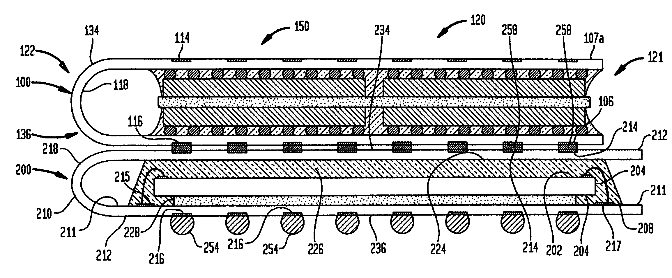
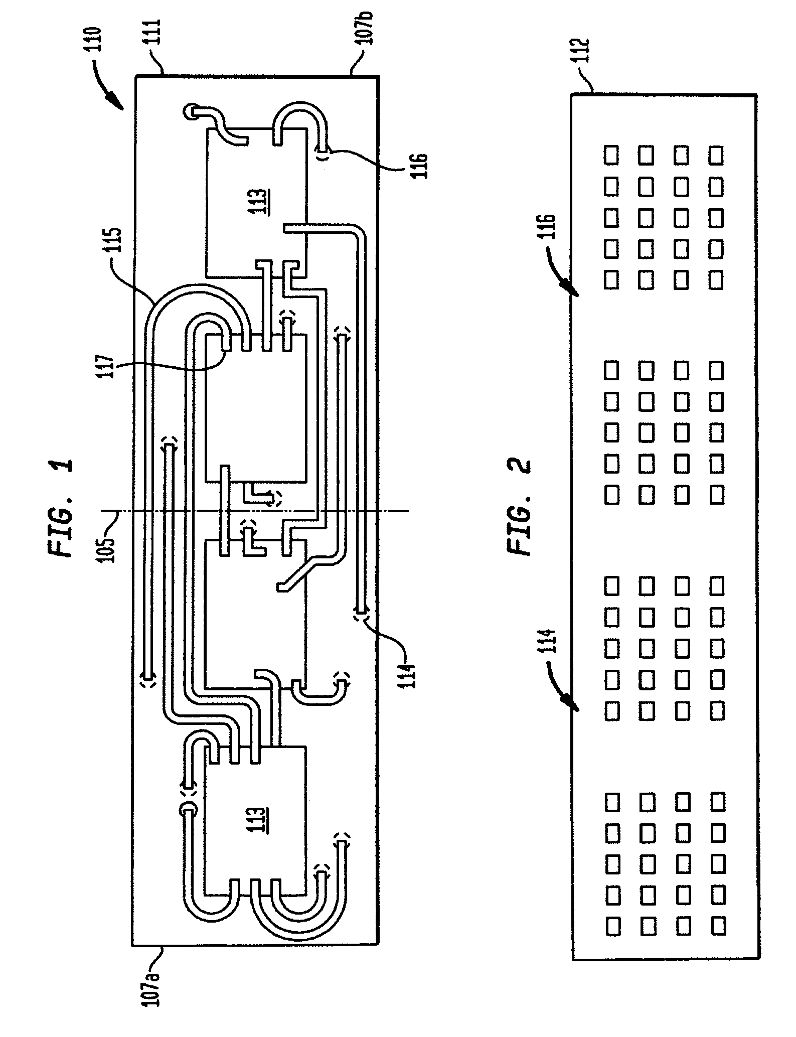
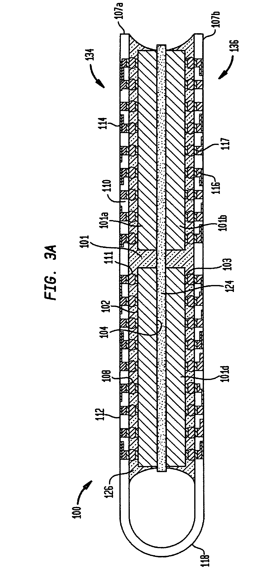
[0040]An embodiment of the invention is shown in FIGS. 1–3A and 4. Substrate 110 comprises an elongated dielectric sheet having a first end 107a and a second end 107b. Substrate 110 is desirably flexible and has a plurality of attachment sites 113 on the first side 111 as best seen in FIG. 1 and first contacts 116 and second contacts 114 disposed at or near a second side 112 as best seen in FIG. 2. Substrate 110 includes a wiring layer with flexible leads 115 extending to the attachment sites 113. Through holes, vias, or other conductive members extend between the contacts to the flexible leads 115 at or near the first side 111 of the substrate 110. The flexible leads 115 have pads 117 exposed at or within the attachment sites 113. Some of the leads 115 extend between pads 117 and the first contacts 116 and some extend between pads 117 and second contacts 114. Some leads 115 extend between two pads 117 at two different attachment sites 113. Some leads extend between first contacts 1...


PUM


Abstract

A stacked microelectronic assembly includes a plurality of microelectronic subassemblies. Each subassembly includes a substrate having at least one site, a plurality of first contacts and a plurality of second contacts. Each subassembly also has at least one microelectronic element assembled to the at least one attachment site and electrically connected to at least some of the first and second contacts. The substrate is folded so that the first contacts are accessible at a bottom of a subassembly and the second contacts are accessible at a top of a subassembly. The plurality of subassemblies are stacked one on top of another in a generally vertical configuration. The substrate of at least one of the subassemblies has a plurality of attachment sites and a plurality of microelectronic elements assembled to the attachment sites. The substrate is folded so that at least some of the plurality of microelectronic elements are disposed alongside one another.

Description

CROSS-REFERENCE TO RELATED APPLICATIONS[0001]This application is a continuation-in-part of application Ser. No. 09 / 776,356, filed Feb. 2, 2001, now U.S. Pat. No. 6,699,730, which is a divisional of application Ser. No. 09 / 244,581, filed Feb. 4, 1999, now U.S. Pat. No. 6,225,688, which is a continuation-in-part of application Ser. No. 08 / 987,569, filed Dec. 11, 1997, now U.S. Pat. No. 6,121,676, claiming benefit of Provisional Application No. 60 / 033,353, filed Dec. 13, 1996, the disclosures of which are all hereby incorporated by reference herein. This application also claims benefit of Provisional Application No. 60 / 343,821, filed Oct. 26, 2001, the disclosure of which is hereby incorporated by reference herein.FIELD OF THE INVENTION[0002]The present invention relates to microelectronic assemblies and, in particular, assemblies wherein a number of subassemblies are stacked one on top of another to form the microelectronic assembly.BACKGROUND OF THE INVENTION[0003]Certain microelectr...

Claims


Application Information

Patent Timeline
Patent Type & Authority Patents(United States)
IPC IPC(8): H05K1/11H01L23/538H01L25/065H05K1/18
CPCH01L23/5387H01L25/0657H05K1/189H01L2225/06517H01L2225/0652H01L2225/06541H01L2225/06555H01L2225/06579H01L2225/06582H01L2225/06586H01L2924/3011H01L2224/16H01L2224/05573H01L2224/05568H01L2924/00014H01L2224/05599
Inventor WARNER, MICHAELDAMBERG, PHILIPRILEY, JOHN B.GIBSON, DAVIDKIM, YOUNG-GONHABA, BELGACEMSOLBERG, VERNON
Owner TESSERA INC
Why Eureka
Try Eureka