Active matrix liquid crystal display

a liquid crystal display and active matrix technology, applied in the direction of instruments, static indicating devices, etc., can solve the problems of delay in the response of liquid crystals, deteriorating dynamic image resolution, etc., and achieve the effect of secure dynamic image resolution

Active Publication Date: 2007-03-20
JVC KENWOOD CORP
View PDF16 Cites 22 Cited by
  • Summary
  • Abstract
  • Description
  • Claims
  • Application Information

AI Technical Summary

Benefits of technology

[0014]An object of the present invention is to provide an active matrix LCD that writes display signals in each row of pixels of the LCD in a first part of a frame period (vertical scan period) and resets each row of the pixels to a reset voltage in a second part of the frame period, to thereby secure dynamic image resolution.
[0015]Another object of the present invention is to provide an active matrix LCD employing a simple structure to optionally set a display signal period and a reset period in each frame period, to satisfy different system requirements and realize different display modes such as a “brightness priority” mode and a “dynamic image characteristic priority” mode.

Problems solved by technology

This results in blurring the second frame image and deteriorating dynamic image resolution.
Such a delay in the response of liquid crystals deteriorates dynamic image resolution.

Method used


Image

  • Active matrix liquid crystal display
  • Active matrix liquid crystal display
  • Active matrix liquid crystal display

Examples


Embodiment Construction

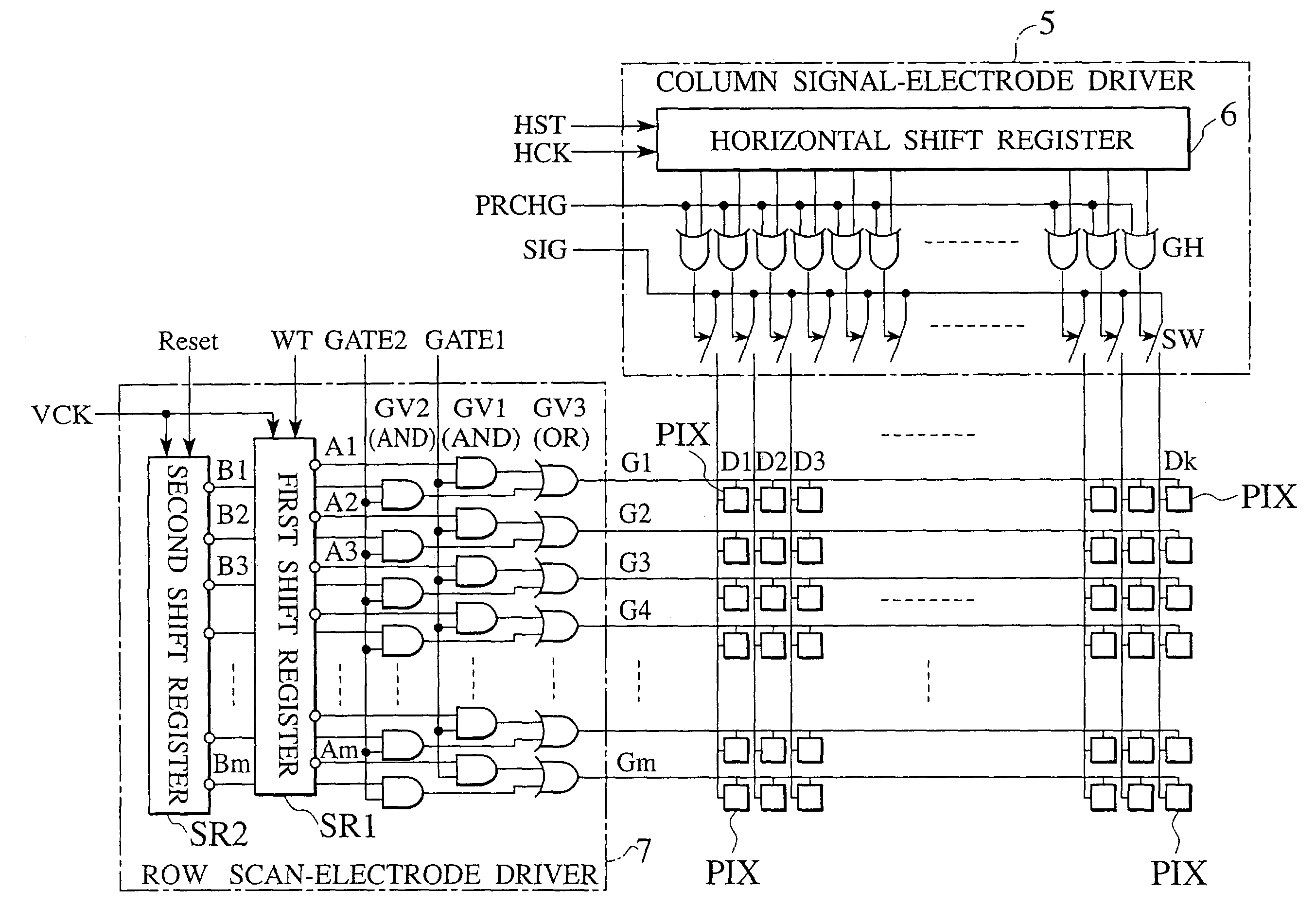
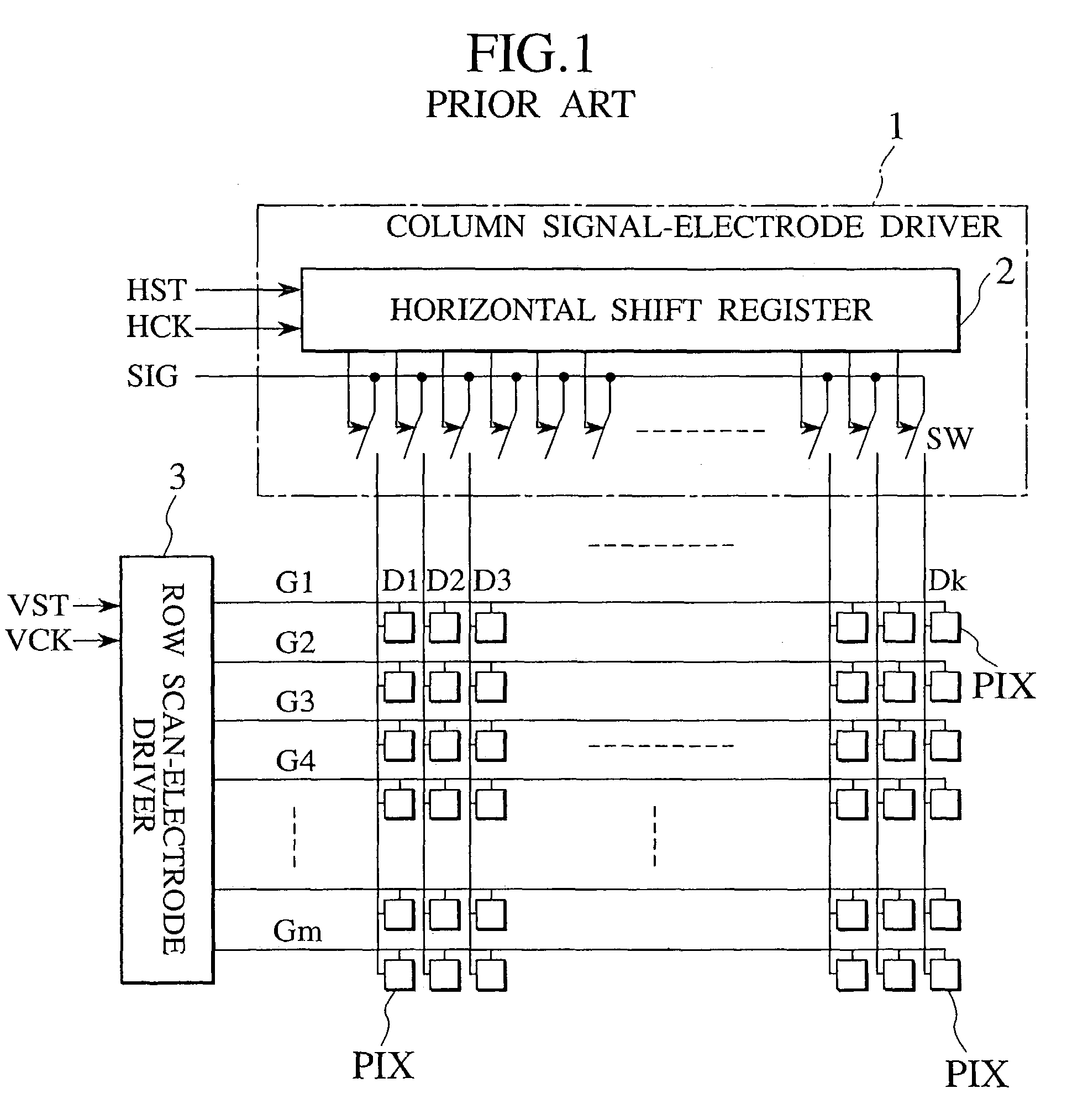
[0031]Embodiments of the present invention will be explained with reference to the accompanying drawings. FIG. 3 is a circuit diagram showing an active matrix LCD according to an embodiment of the present invention. The LCD includes column signal-electrodes D1 to Dk and row scan-electrodes G1 to Gm that are orthogonal to the column signal-electrodes D1 to Dk. At each intersection of the column signal-electrodes and row scan-electrodes, a pixel PIX is formed. The pixels PIX are arranged in a two-dimensional matrix.

[0032]The column signal-electrodes D1 to Dk are driven by a column signal-electrode driver 5. The column signal-electrode driver 5 has a horizontal shift register 6, a switch group SW, and a gate group GH. The gate group GH consists of k two-input OR gates. The horizontal shift register 6 has k bit-output terminals that are connected to first input terminals of the two-input OR gates, respectively. Second input terminals of the two-input OR gates are commonly connected to a...


PUM

PropertyMeasurementUnit
reset voltageaaaaaaaaaa
voltageaaaaaaaaaa
drive voltageaaaaaaaaaa

Abstract

An active matrix LCD defines a display signal period and a reset period in each vertical scan period. The display signal period is a period to write and hold display signals in pixels in response to a row select pulse generated from an output pulse of a first shift register (SR1). The reset period is a period to write and hold a reset voltage in the pixels in response to a row select pulse generated from an output pulse of a second shift register (SR2). The ratio of the display signal period to the reset period is adjustable in units of horizontal scan time by changing the number “n” of horizontal scan periods to be passed between the time when the first shift register receives a scan start signal (WT) and the time when the second shift register receives a scan start signal (Reset).

Description

BACKGROUND OF THE INVENTION[0001]1. Field of the Invention[0002]The present invention relates to an active matrix liquid crystal display, and particularly, to that suitable for a projection liquid crystal display.[0003]2. Description of Related Art[0004]FIG. 1 is a schematic view showing an example of an active matrix, LCD (liquid crystal display) according to a related art. The LCD has column electrodes D1 took for display signals and row electrodes G1 to Gm for scanning. The row scan-electrodes G1 to Gm are orthogonal to the column signal-electrodes D1 to Dk. At each intersection of the column signal-electrodes and row scan-electrodes, a pixel PIX is formed. The pixels PIX are arranged in a two-dimensional matrix.[0005]The column signal-electrodes D1 to Dk are driven by a column signal-electrode driver 1 having a horizontal shift register 2 and a group of switches SW. The shift register 2 has output stages connected to control terminals of the switches SW, respectively. Input term...

Claims


Application Information

Patent Timeline
Patent Type & Authority Patents(United States)
IPC IPC(8): G09G3/36G09G3/20G02F1/133
CPCG09G3/3677G09G3/3688G09G3/2011G09G2300/0842G09G2320/0252G09G2310/0267G09G2310/0275G09G2310/061G09G2310/062G09G2310/0254
Inventor FURUYA, MASATO
Owner JVC KENWOOD CORP
Why Eureka
Try Eureka