Method and apparatus for real time identification and correction of pixel defects for image sensor arrays

a technology of image sensor array and real-time identification, applied in image enhancement, color signal processing circuit, instruments, etc., can solve the problems of limited number of defects that can be corrected, the effect of affecting a significant portion of the image is compounded, and the defect location is required. , to achieve the effect of reducing peak-to-peak noise variations in the imag

Active Publication Date: 2007-04-10
APTINA IMAGING CORP
View PDF24 Cites 29 Cited by
  • Summary
  • Abstract
  • Description
  • Claims
  • Application Information

AI Technical Summary

Benefits of technology

[0009]The present invention addresses the disadvantages of the prior art by providing a method and apparatus which enables real time correction of image data for an arbitrary number of both dark and bright defective pixels in an image sensor array without the need for a separate production-stage calibration to account for the defective pixels or a non-volatile medium to store a pre-calibrated defect map. The method and apparatus of the invention also enables the identification of defective pixel data without relying on a specific definition of a defect and without requiring the use of any specified thresholds against which potential defects are compared. The method and apparatus of the invention also enables correction of defective pixel data in an image regardless of the image contents and the correction of defective pixel data in an image without appreciably affecting the resolution of the image, and the correction of defective pixel data in an image, while also reducing peak-to-peak noise variations in the image.

Problems solved by technology

Thus, when a pixel is defective, its effects can be compounded to affect a significant portion of the image.
Due to a number of inherent variabilities in the manufacturing processes of image sensors such as charge-coupled devices (CCDs) or complementary metal oxide semiconductors (CMOSs), some of the pixels of the imaging array in each sensor are either always dark (often due to a short in the circuitry) or always too bright (often due to abnormally high leakage current).
However, this substitution requires knowledge of the defective pixel locations.
The main drawback of this conventional approach is that the number of defects that can be corrected is limited by the size of the non-volatile memory dedicated to this purpose.
Another drawback of the conventional approach is that it requires a separate manufacturing step for the identification and storage of the defect locations.

Method used


Image

  • Method and apparatus for real time identification and correction of pixel defects for image sensor arrays
  • Method and apparatus for real time identification and correction of pixel defects for image sensor arrays
  • Method and apparatus for real time identification and correction of pixel defects for image sensor arrays

Examples


Embodiment Construction

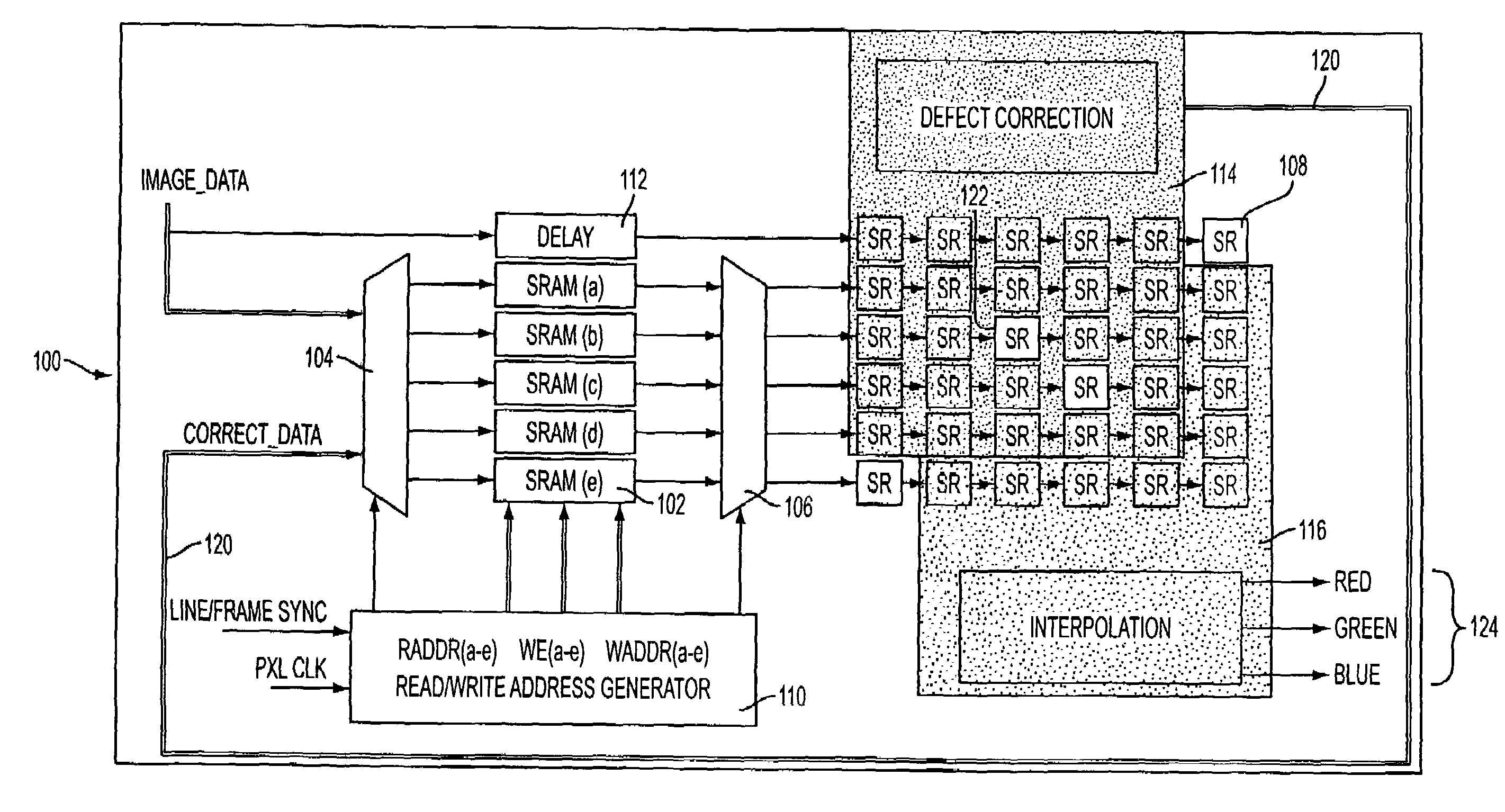
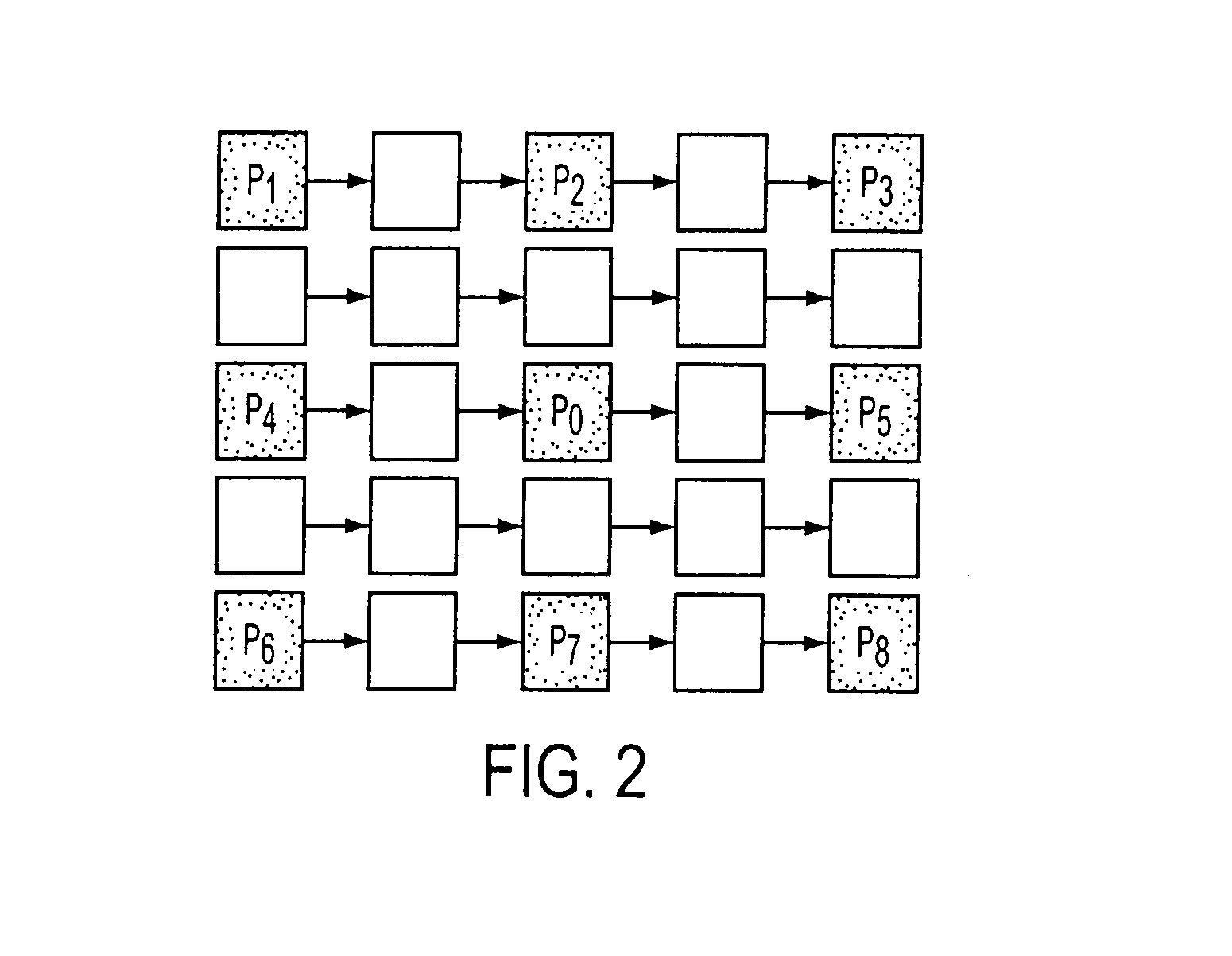
[0019]In the method aspect of the present invention, the signal value of each pixel in an image obtained by an image sensor is compared with the values for at least eight closest surrounding pixels having the same color filter located adjacent to or near the pixel being tested. An example of this method will be described for an image obtained by an image sensor having a Bayer mosaic filter array. As illustrated in FIG. 2, the signal value of the central pixel, P0, is compared with the signal values for each of the eight closest surrounding pixels of the same color. In this example, these eight closest surrounding pixels are located along the same row (P4, P5), column (P2, P7), and diagonally (P1, P3, P6, and P8) from the pixel being tested (P0), each spaced one pixel away from P0 in the relevant direction.

[0020]If the signal of P0 is larger than the respective signals of all eight surrounding pixels P1 through P8, then the signal value for P0 is substituted with the maximum signal v...


PUM


Abstract

An image processing system and method compares each pixel of an image obtained from an image sensor array with at least eight surrounding pixels of the same color in the filter array. If the signal of a given pixel is larger than the respective signals of all eight surrounding pixels of the same color, then the value of that central pixel signal is substituted with the maximum signal value among the surrounding eight pixels of the same color. Similarly, if the signal of a given pixel is smaller than the respective signals of all eight surrounding pixels of the same color, then the value of that central pixel signal is substituted with the minimum signal value among the surrounding eight pixels of the same color.

Description

FIELD OF THE INVENTION[0001]The present invention relates to a method and apparatus that enables real time identification and correction of defective pixels in an image sensor array in a digital imaging environment.BACKGROUND OF THE INVENTION[0002]When an image is exposed onto an image sensor, each pixel records the amount of light that it “sees” as an intensity level between a dark signal wherein no light reaches that pixel, to a full white signal representing the maximum amount of light detectable by that pixel. The image thus captured by the image sensor is processed as a grayscale image.[0003]To detect the colors of the image exposed onto the image sensor, the pixels of the image sensor are covered with a respective color filter that absorbs light wavelengths for all colors except the color of the filter. An exemplary method for acquiring color information from an image sensor is to place a color filter array over the pixels of an image sensor. The most common example of such a ...

Claims


Application Information

Patent Timeline
Patent Type & Authority Patents(United States)
IPC IPC(8): H04N9/64H04N5/21H04N5/213H04N5/217H04N5/357H04N5/367H04N5/369H04N9/07
CPCH04N5/3675G06T5/005G06T5/20H04N25/683H04N9/64H04N25/60
Inventor KAPLINSKY, MICHAELSUBBOTIN, IGOR
Owner APTINA IMAGING CORP
Why Eureka
Try Eureka