Plasma display panel including dielectric layer that does not cover part of a discharge gap

a dielectric layer and plasma display technology, applied in the field can solve the problems of limited discharge gap size, low brightness and luminous efficiency of plasma display panels, and inability to freely expand the discharge gap,

Inactive Publication Date: 2007-07-03
PANASONIC CORP
View PDF19 Cites 10 Cited by
  • Summary
  • Abstract
  • Description
  • Claims
  • Application Information

AI Technical Summary

Problems solved by technology

However, brightness and luminous efficiency of plasma display panels remain low, so that current plasma display panels have only approximately ⅓ the luminous efficiency of a CRT, which is popular as a display apparatus.
However, a size of a pixel is determined by the necessary number of pixels and a screen size of the display device, so that the size of the discharge gap is restricted by the size of the pixel and can not be freely enlarged.

Method used


Image

  • Plasma display panel including dielectric layer that does not cover part of a discharge gap
  • Plasma display panel including dielectric layer that does not cover part of a discharge gap
  • Plasma display panel including dielectric layer that does not cover part of a discharge gap

Examples


first embodiment

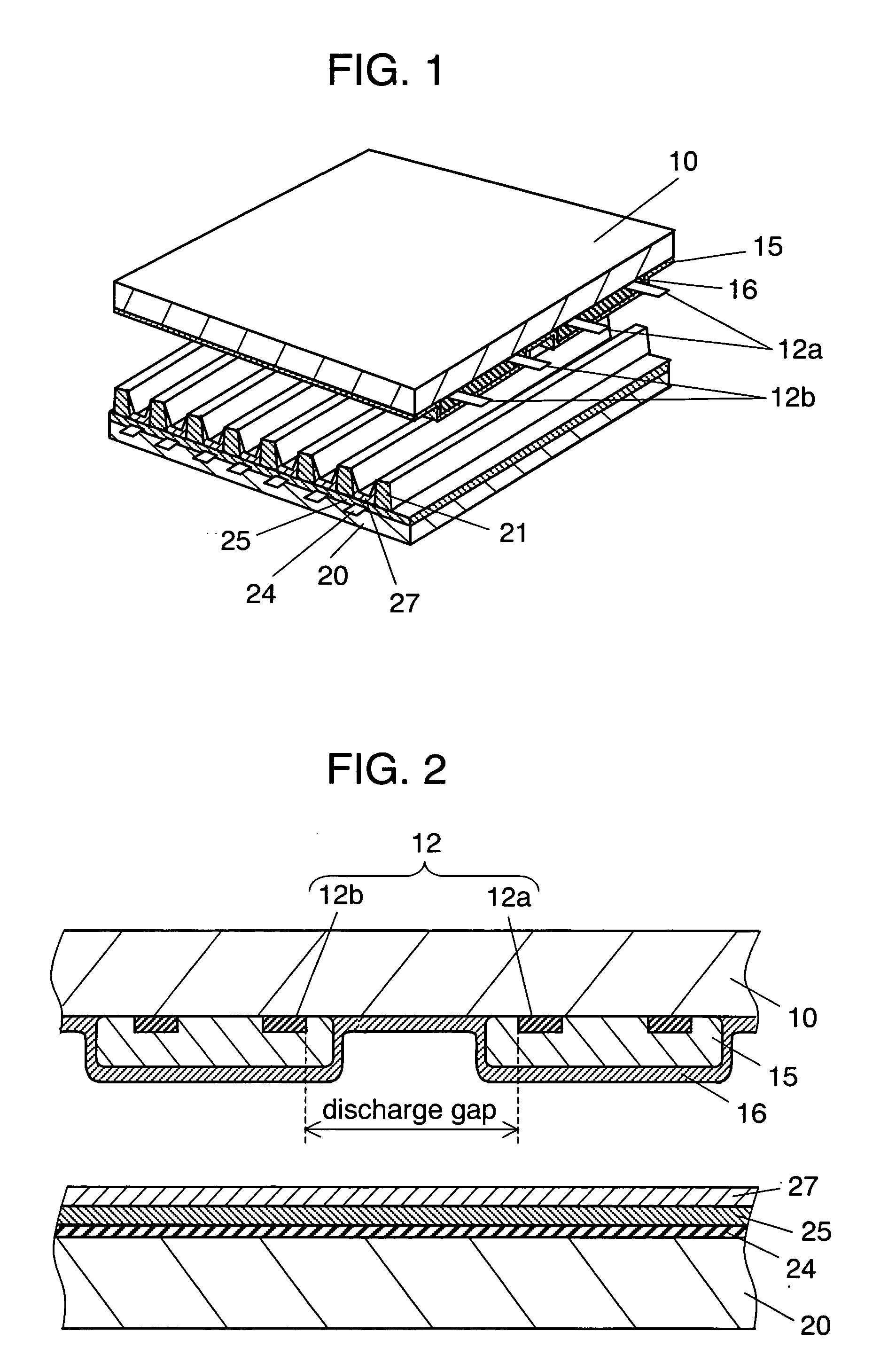
[0019]FIG. 1 is an exploded perspective view showing a structure of a plasma display panel in accordance with the first exemplary embodiment of the present invention. FIG. 2 is a sectional view showing the structure of the plasma display panel in accordance with the first exemplary embodiment of the present invention.

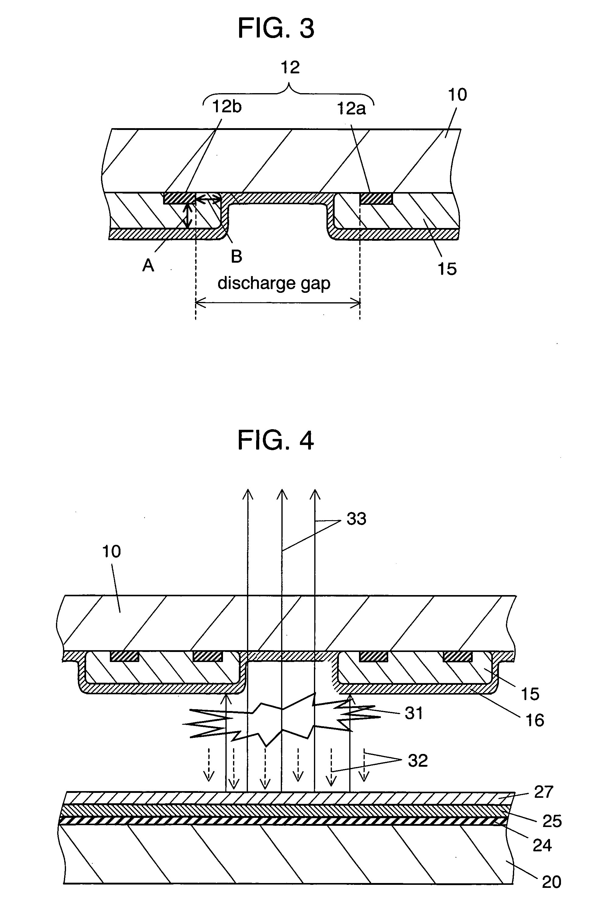
[0020]Display electrodes 12 (i.e., a pair of display electrodes 12a and 12b) are disposed parallel to each other on front substrate 10, thereby forming a discharge gap for emitting light for display. Each of display electrodes 12a and 12b is covered with dielectric layer 15. However, the discharge gap formed between display electrodes 12a and 12b is not covered with dielectric layer 15. Protective layer 16 covers dielectric layer 15 and the discharge gap. In other words, the discharge gap is not covered with dielectric layer 15, and is directly covered with protective layer 16.

[0021]A plurality of data electrodes 24 and barrier ribs 21 are alternately disposed on rear s...

second embodiment

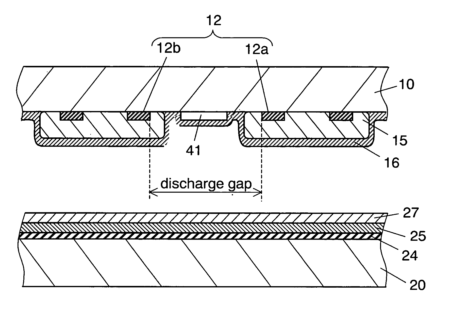
[0029]FIG. 5 is a sectional view showing a structure of a plasma display panel in accordance with the second exemplary embodiment of the present invention. FIG. 6 is a plan view showing the structure of the plasma display panel in accordance with the second exemplary embodiment of the present invention. The plasma display panel in the second embodiment is identical with that in the first embodiment in that a discharge gap formed between display electrodes 12a and 12b is not covered with dielectric layer 15. However, the plasma display panel in the second embodiment differs from that in the first embodiment in that float electrode 41, which is electrically insulated from display electrodes 12, is formed at the discharge gap where dielectric layer 15 is not formed. Protective layer 16 is formed in a manner to cover float electrode 41 and dielectric layer 15.

[0030]Float electrode 41 is made of electrically conductive material, such as an SnO2 layer or an ITO layer, which is transparent...


PUM


Abstract

An AC type plasma display panel includes a plurality of pairs of display electrodes, a dielectric layer, a data electrode and a float electrode. A pair of the plurality of pairs of display electrodes are disposed parallel to each other on a front substrate and form a discharge gap for emitting light for display. The dielectric layer is formed on the front substrate and covers the plurality of pairs of display electrodes excluding at least a part of the discharge gap. The data electrode is disposed on a rear substrate, which is placed facing the front substrate across a discharge space, in a manner to cross under the display electrodes. The float electrode is disposed at the discharge gap on the front substrate.

Description

FIELD OF THE INVENTION[0001]The present invention relates to a plasma display panel which can display an image with high brightness and high efficiency.BACKGROUND OF THE INVENTION[0002]A plasma display panel is a display device having superior visibility and characterized by its thinness, lightness and large display. The plasma display panels are classified into two driving systems, i.e., an AC type and a DC type, and classified into two electric discharge systems, i.e., a surface discharge type and an opposed discharge type. The AC and surface discharge type plasma display panel is becoming a mainstream, because it is suitable for high resolution and is easy to manufacture.[0003]However, brightness and luminous efficiency of plasma display panels remain low, so that current plasma display panels have only approximately ⅓ the luminous efficiency of a CRT, which is popular as a display apparatus. Accordingly, various plasma display panels have been developed for the purpose of high b...

Claims


Application Information

Patent Timeline
Patent Type & Authority Patents(United States)
IPC IPC(8): H01J17/49
CPCH01J11/12H01J11/30H01J11/38H01J2211/326
Inventor YUKI, HARUHIROHONMA, YOSHIYASU
Owner PANASONIC CORP
Why Eureka
Try Eureka