
Nozzle apparatus for stripping edge bead of wafer

a technology of edge beads and nozzles, which is applied in the direction of photomechanical apparatus, cleaning using liquids, instruments, etc., can solve the problems of requiring excessive time to remove edge beads, damage to important wafer patterns, and cleaning solutions that may not adequately remove edge beads, etc., to achieve the effect of removing the edge bead of a wafer more quickly and effectively

Inactive Publication Date: 2008-02-12
SAMSUNG ELECTRONICS CO LTD
View PDF22 Cites 7 Cited by
  • Summary
  • Abstract
  • Description
  • Claims
  • Application Information

AI Technical Summary

Benefits of technology

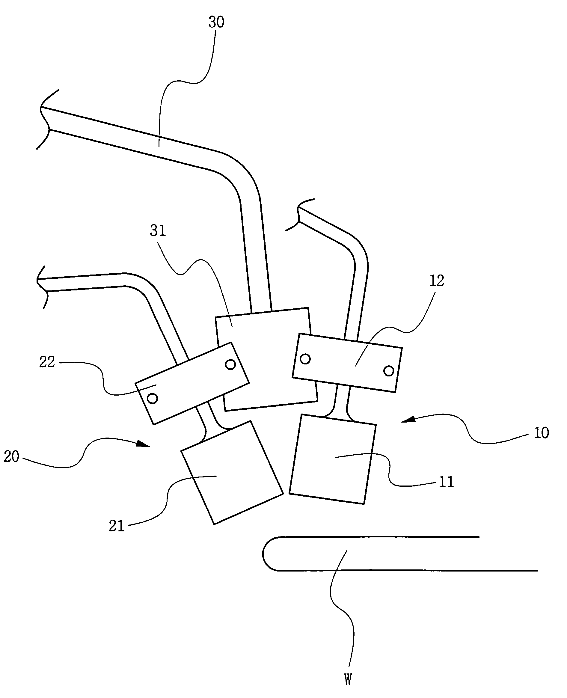
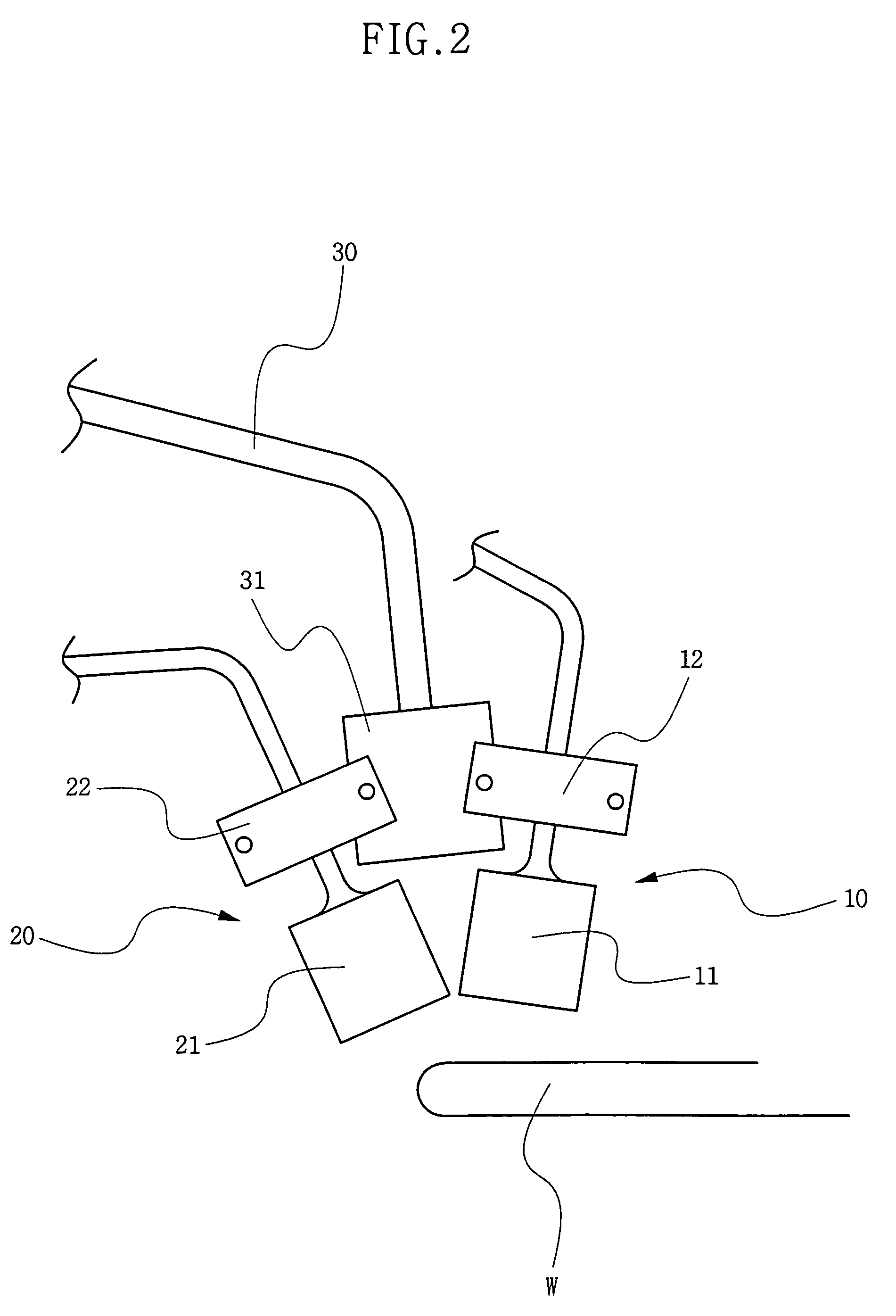
[0012]Therefore, the present invention is directed to a nozzle that sprays a cleaning solution for bead removal and that simultaneously and selectively cleans the upper surface and the outer end surface of a wafer edge, thereby removing the bead of a wafer edge more rapidly and effectively.

Problems solved by technology

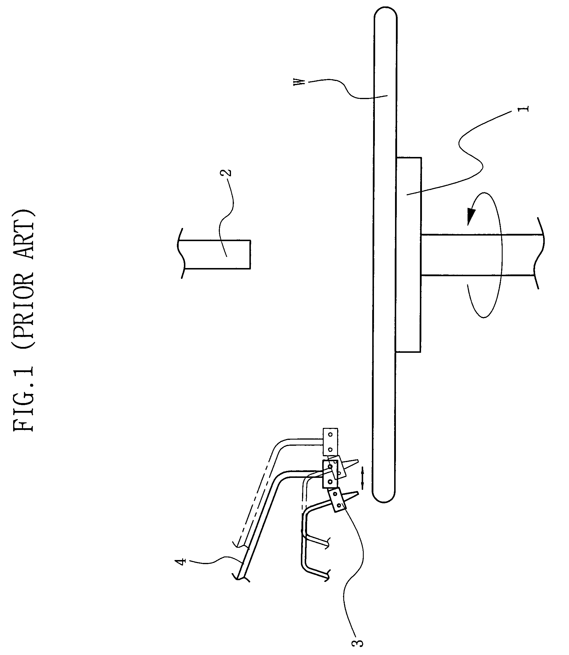
Unfortunately, conventional side rinse nozzles that spray cleaning solution can require excessive time to remove edge beads.
Moreover, extended spray time can damage important patterns of a wafer.
In addition, conventional side rinse nozzles that spray cleaning solution may not adequately remove edge beads.

Method used


Image

  • Nozzle apparatus for stripping edge bead of wafer
  • Nozzle apparatus for stripping edge bead of wafer
  • Nozzle apparatus for stripping edge bead of wafer

Examples


Embodiment Construction

[0022]The present invention now is described more fully hereinafter with reference to the accompanying drawings, in which preferred embodiments of the invention are shown. This invention may, however, be embodied in many different forms and should not be construed as limited to the embodiments set forth herein; rather, these embodiments are provided so that this disclosure will be thorough and complete, and will fully convey the scope of the invention to those skilled in the art.

[0023]Like numbers refer to like elements throughout. In the figures, the thickness of certain lines, layers, components, elements or features may be exaggerated for clarity. Broken lines illustrate optional features or operations unless specified otherwise. All publications, patent applications, patents, and other references mentioned herein are incorporated herein by reference in their entireties.

[0024]The terminology used herein is for the purpose of describing particular embodiments only and is not inten...


PUM


Abstract

There is provided a nozzle apparatus for stripping an edge bead from a wafer, which includes a rotatable support arm, and a side rinse nozzle coupled to a leading end of the support arm to remove the bead of photoresist remaining on the edge of a wafer. The side rinse nozzle has a first nozzle for removing the bead on the upper surface of the wafer edge, and a second nozzle for removing the bead on the outer end surface of the wafer. The first and second nozzles each have a shape such that a length thereof is long in a radial direction of the wafer and a width thereof is narrow.

Description

CROSS-REFERENCE TO RELATED APPLICATION[0001]This application claims the benefit of Korean Patent Application No. 10-2004-0099083, filed Nov. 30, 2004, the disclosure of which is hereby incorporated herein by reference in its entirety.FIELD OF THE INVENTION[0002]The present invention relates generally to semiconductor manufacturing and, more particularly, to semiconductor manufacturing apparatus.BACKGROUND OF THE INVENTION[0003]Generally, a process for manufacturing semiconductor products includes forming, on a pure silicon wafer, a semiconductor chip, packaging the semiconductor chip so as to protect same from external environments while allowing same to electrically communicate with an external device, and testing the packaged semiconductor product.[0004]The step of manufacturing a semiconductor chip includes a sub-step of applying a photoresist of a certain thickness on a wafer surface and performing thereto an exposure and develop process using a mask with a certain pattern, ther...

Claims


Application Information

Patent Timeline
Patent Type & Authority Patents(United States)
IPC IPC(8): B08B3/00
CPCB05C11/08B05C11/10B08B3/02H01L21/6708Y10S134/902B05B1/14B05B13/0228G03F7/2028G03F7/422
Inventor KIM, KYOUNG-HO
Owner SAMSUNG ELECTRONICS CO LTD
Learn More