Architecture for face-to-face bonding between substrate and multiple daughter chips

a technology of face-to-face bonding and substrate, which is applied in the direction of solid-state devices, pulse techniques, basic electric elements, etc., can solve the problems of unneeded gates, unsatisfactory i/o solutions for customers, and unsatisfactory solutions for industry

Active Publication Date: 2008-04-15
MICROSEMI SOC
View PDF13 Cites 216 Cited by
  • Summary
  • Abstract
  • Description
  • Claims
  • Application Information

AI Technical Summary

Problems solved by technology

A secondary cost issue is that often customers may need a significant amount of I / O and not many gates.
Another problem is that some manufacturers envision creating a number of system-on-a-chip (SOC) integrated circuits and derivatives that employ FPGA and other programmable logic technology.
In addition, the number of FPGA gates needed for each set of peripherals will be customer dependent, again creating a situation where the customer is paying for un-needed gates.
The industry has not come up with a good solution for the I / O problem to date.
This solution however requires flip-chip packaging.
None of these variations are employing 3D packaging to solve the above-described I / O problem.

Method used


Image

  • Architecture for face-to-face bonding between substrate and multiple daughter chips
  • Architecture for face-to-face bonding between substrate and multiple daughter chips
  • Architecture for face-to-face bonding between substrate and multiple daughter chips

Examples


Embodiment Construction

[0018]Persons of ordinary skill in the art will realize that the following description of the present invention is illustrative only and not in any way limiting. Other embodiments of the invention will readily suggest themselves to such skilled persons.

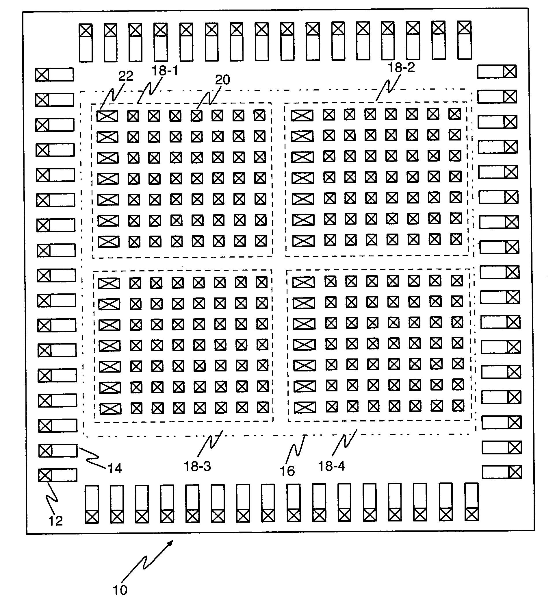
[0019]The present invention employs a low-cost substrate to carry face-to-face mounted daughter chips which can be fabricated in a high-cost state-of-the-art process. The idea is to build an FPGA family in a modular fashion in order to save research and development and non-recurring engineering costs while providing a way to nimbly create derivative parts in response to market conditions.

[0020]The I / O circuit portion of an FPGA can be manufactured on mature processes because, among other reasons, a system designer requires higher voltages for signals sent off-chip (e.g., to other components on a printed circuit) board signaling than that needed for the FPGA core. Wafer prices for circuits manufactured using such mature processes are t...


PUM


Abstract

An integrated circuit system includes a first integrated circuit die and a family of second integrated circuit dice. The first integrated circuit die have input / output circuits disposed thereon and further have a first array of face-to-face bonding structures disposed on a first face thereof. Each member of the family of second integrated circuit dice have logical function circuits disposed thereon and further have a second array of face-to-face bonding structures disposed on a first face thereof. The second array of face-to-face bonding structures of each member of the family mates with a different portion of the first array of face-to-face bonding structures.

Description

RELATED APPLICATIONS[0001]This application is a continuation-in-part of co-pending application Ser. No. 10 / 955,929, filed Sep. 29, 2004, entitled “FACE-TO-FACE BONDED I / O CIRCUIT DIE AND FUNCTIONAL LOGIC CIRCUIT DIE SYSTEM” and assigned to the same assignee as the present invention.BACKGROUND OF THE INVENTION[0002]1. Field of the Invention[0003]The present invention relates to user-programmable integrated circuits. More particularly, the present invention relates to a substrate architecture for face-to-face bonding to multiple daughter chips.[0004]2. The Prior Art[0005]As process geometries scale, the portion of the area of digital-logic function integrated circuits such as field-programmable-gate-array (FPGA) integrated circuits and mixed digital and analog function integrated circuits that must be devoted to input / output (I / O) represents an increasing percentage of the die area relative to logic gates. A secondary cost issue is that often customers may need a significant amount of...

Claims


Application Information

Patent Timeline
Patent Type & Authority Patents(United States)
IPC IPC(8): H01L23/02
CPCH01L25/18H03K19/17732H03K19/17744H03K19/17796H01L2224/16145H01L2225/0651H01L2225/06513H01L2224/05573H01L2924/00014H01L2224/0554H01L24/06H01L2224/06136H01L24/05H01L2224/05599H01L2224/0555H01L2224/0556H01L2224/05568
Inventor PLANTS, WILLIAM C.MCCOLLUM, JOHNSPEERS, THEODORE
Owner MICROSEMI SOC
Why Eureka
Try Eureka