

Multiprocessor node controller circuit and method
a node controller and multi-processor technology, applied in data switching networks, memory address/allocation/relocation, instruments, etc., can solve the problems of difficult to enforce a deterministic order of events when necessary in such a system, and achieve the effect of facilitating high-speed processing and superior performance-cost benefits
- Summary
- Abstract
- Description
- Claims
- Application Information
AI Technical Summary
Benefits of technology
Problems solved by technology
Method used
Image

Examples
Embodiment Construction
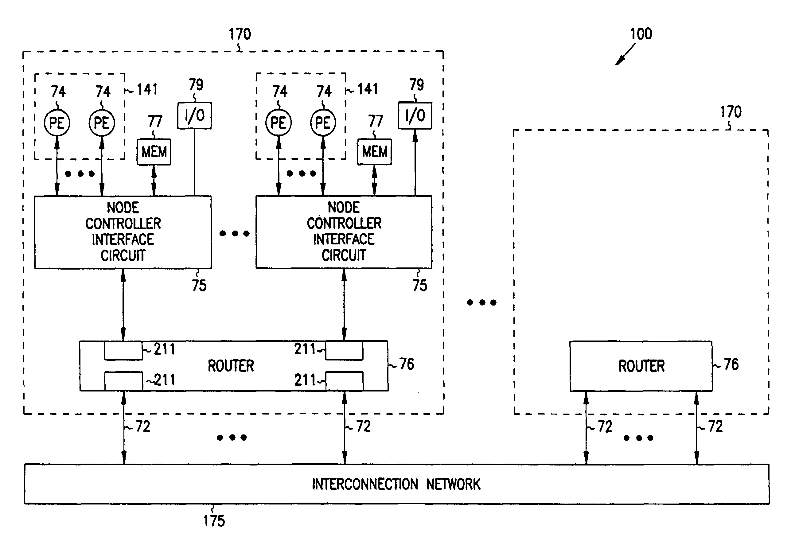
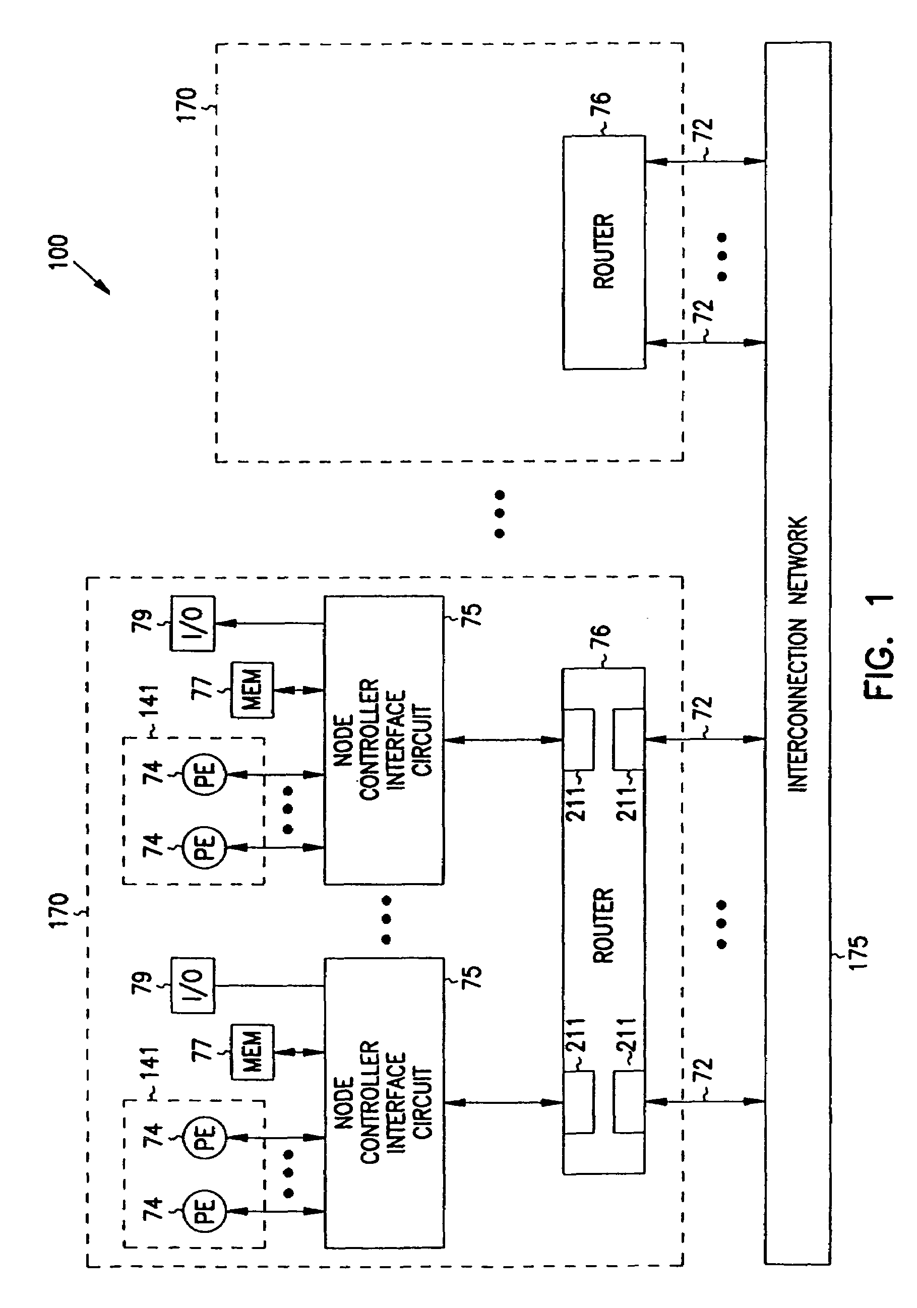
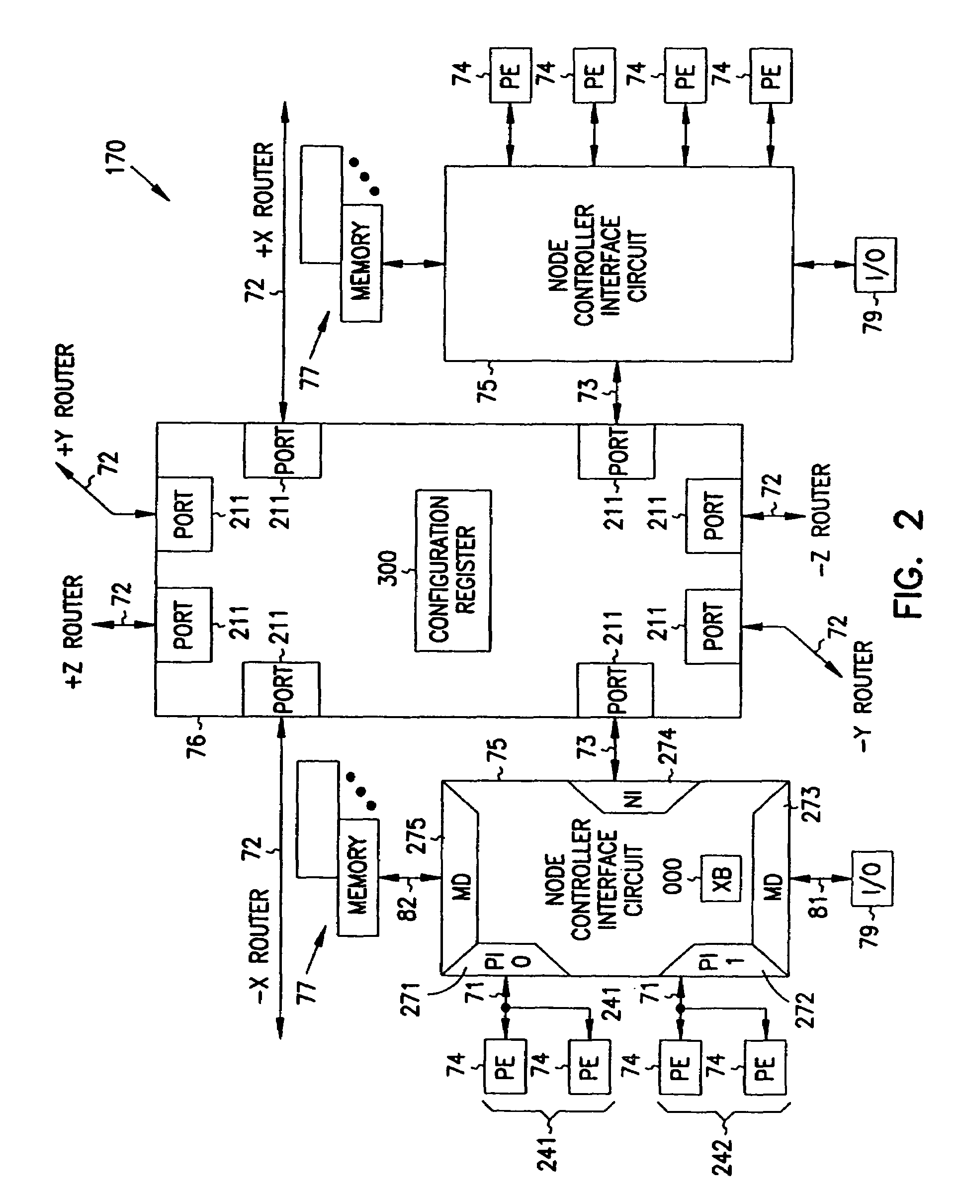
[0088]In the following detailed description of the preferred embodiments, reference is made to the accompanying drawings that form a part hereof, and in which are shown by way of illustration specific embodiments in which the invention may be practiced. It is understood that other embodiments may be utilized and structural changes may be made without departing from the scope of the present invention.
[0089]Some embodiments of the present invention include routers, networks, and synchronization apparatus and methods as described further in copending U.S. patent application Ser. No. 08 / 972,010 filed Nov. 17, 1997, which is hereby incorporated by reference.
[0090]Some embodiments implement multiprocessor systems, that generally do not use a coherent cache model. Other embodiments include cache coherence mechanisms and methods such as described in application Ser. No. 08 / 971,184 filed Nov. 17, 1997 entitled “MULTI-DIMENSIONAL CACHE COHERENCE DIRECTORY STRUCTURE”, which is hereby incorpora...
PUM
 Abstract
Description
Claims
Application Information