Circuit device

a circuit device and circuit technology, applied in the field of circuit devices, can solve the problems of low reliability, high demand for high function and high performance of lsis, and the product must be small and lightweight, so as to reduce the propagation of ground nois

Active Publication Date: 2008-11-18
SEMICON COMPONENTS IND LLC +1
View PDF7 Cites 21 Cited by
  • Summary
  • Abstract
  • Description
  • Claims
  • Application Information

AI Technical Summary

Benefits of technology

[0013]The present invention has been made in view of the foregoing circumstances and a general purpose thereof is to provide a circuit device having a multiple stack structure featuring reduced ground noise propagating between circuit elements thereof.

Problems solved by technology

For them to be accepted by the market, however, such products must be small and lightweight.
On the other hand, what is required of these electronics devices is handiness and ease of use, and consequently the demand is high for the high function and high performance of LSIs used in these devices.
This noise component affecting the lower-layer semiconductor chip via the ground wiring has been a factor of destabilizing the operation of the circuit device, thus causing a drop in reliability.

Method used


Image

  • Circuit device
  • Circuit device
  • Circuit device

Examples


first embodiment

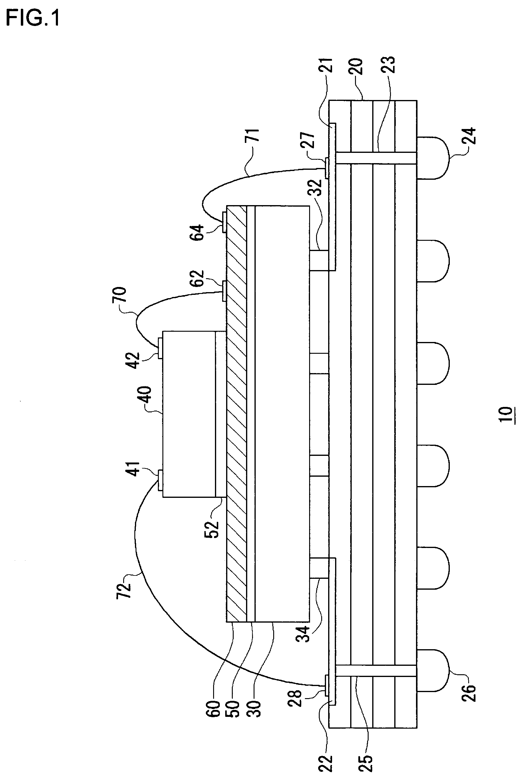
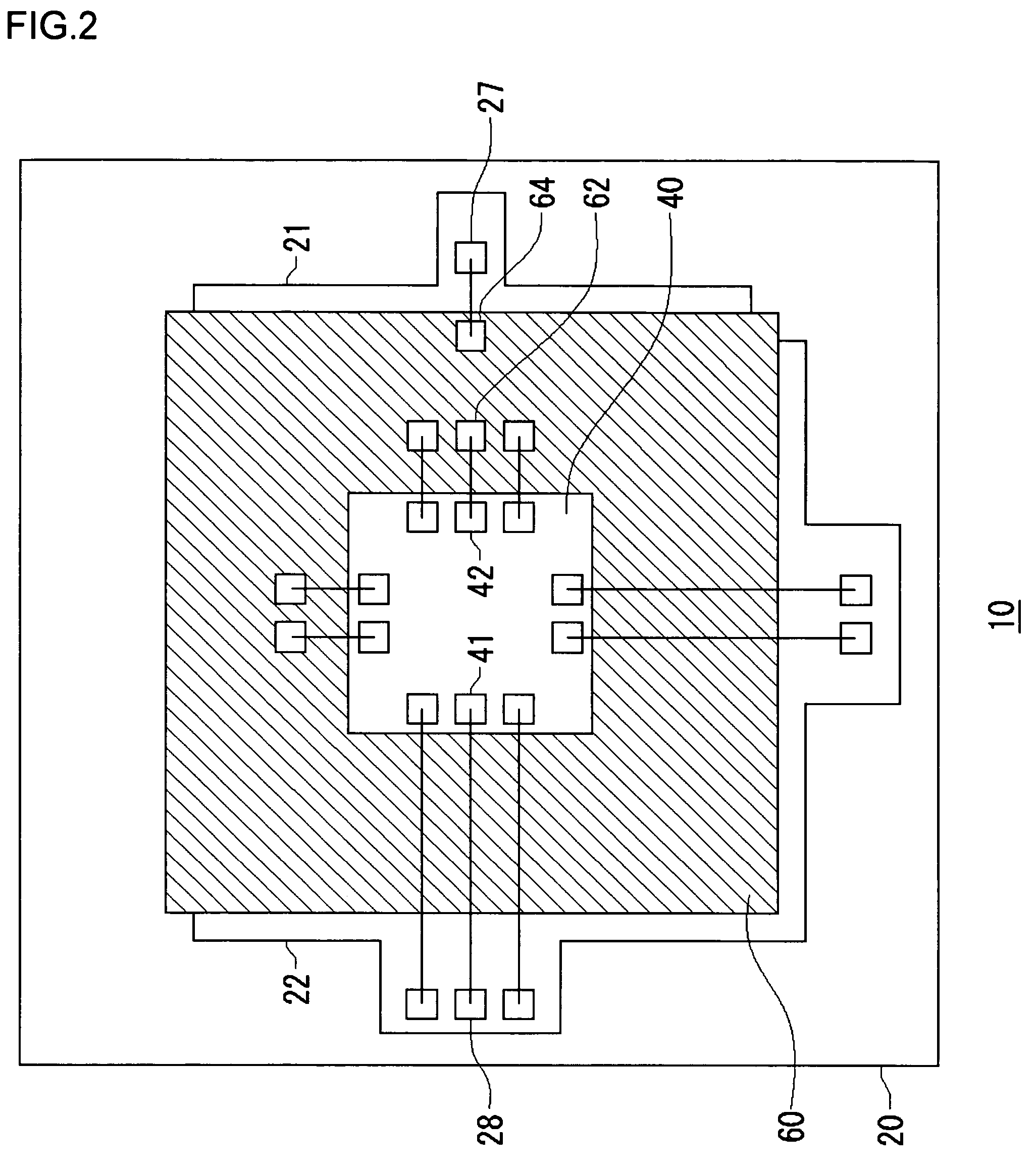
[0047]FIG. 1 is a cross-sectional view showing a structure of a circuit device according to a first embodiment of the present invention. FIG. 2 is a plan view showing a circuit device according to the first embodiment.

[0048]A circuit device 10 according to the first embodiment includes a substrate 20, a first circuit element 30, which is flip-chip-bonded to the substrate 20, a second circuit element 40, which is stacked on top of the first circuit element 30, a pair of insulation layers, namely, an insulation layer 50 and an insulation layer 52, which are interposed between the first circuit element 30 and the second circuit element 40, and a conductive layer 60, which is interposed between the insulation layer 50 and the insulation layer 52.

[0049]The substrate 20 has a multilayer wiring structure of a plurality of stacked wiring layers. Provided on the surface of the substrate 20 are a ground wiring 21 and a power supply wiring 22. The ground wiring 21 is connected to a BGA ball 24...

second embodiment

[0080]FIG. 6 is a cross-sectional view showing a structure of a circuit device 500 according to a second embodiment of the present invention. FIG. 7 is a plan view showing a circuit device according to the second embodiment.

[0081]A circuit device 500 according to the second embodiment differs from the circuit device 10 according to the first embodiment in that the circuit elements of the second embodiment are formed by three stacks. A description will be given here of the circuit device 500 according to the second embodiment centering around a structure different from that of the first embodiment.

[0082]According to the second embodiment, a third circuit element 580 is further laminated on the second circuit element 40. A pair of insulation layers 550 and 570 are provided between the third circuit element 580 and the second circuit element 40. A conductive layer 560 is interposed between the insulation layer 550 and the insulation layer 570.

[0083]A bonding pad 530, for power supply, ...

third embodiment

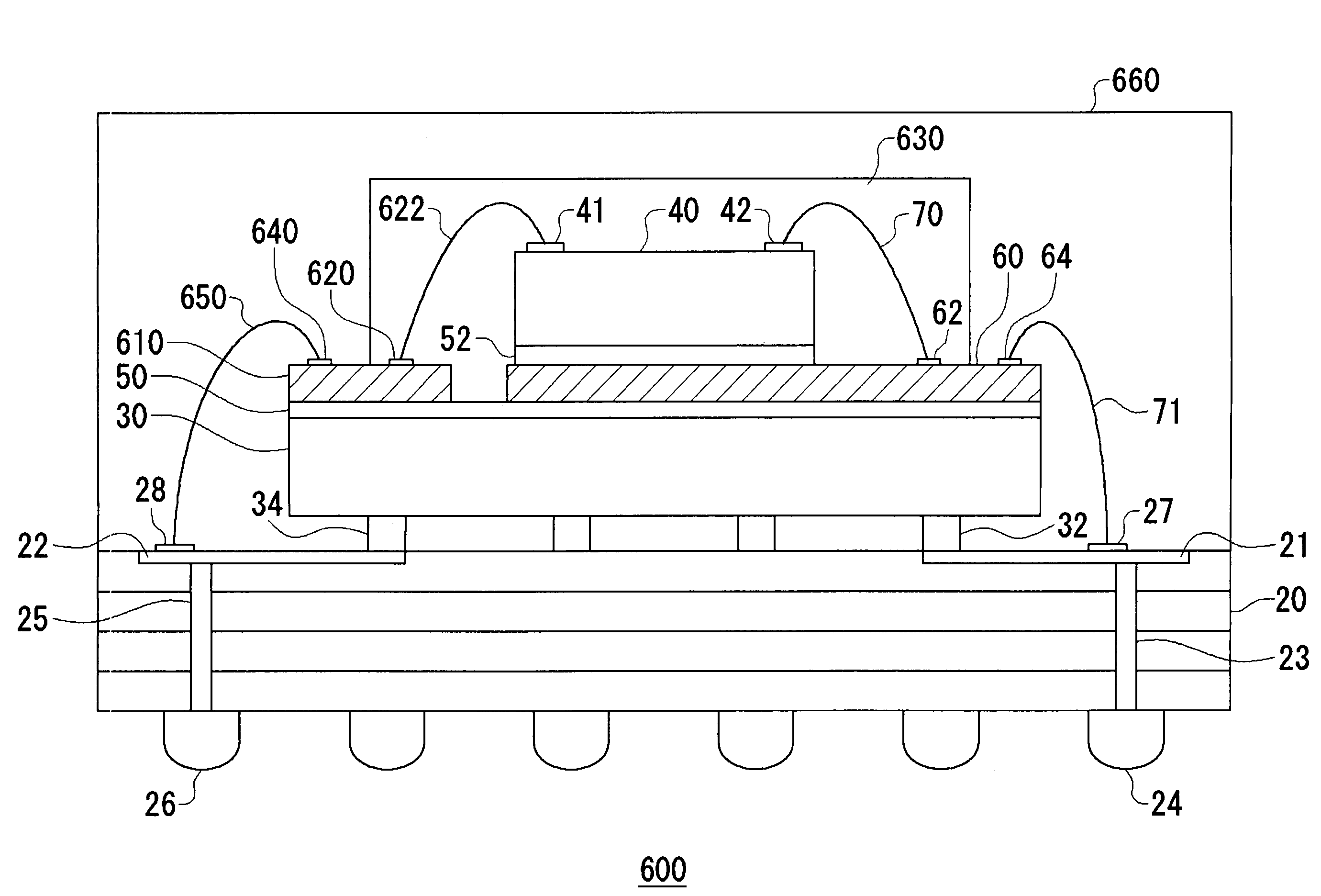
[0086]FIG. 8 is a cross-sectional view showing a structure of a circuit device 600 according to a third embodiment of the present invention. A description will be given hereinbelow of the circuit device 600 according to the third of the first embodiment. A packaged second circuit element 40 is used in the circuit device 600. A first circuit element mounted on a substrate 20 and the packaged second circuit element 40 are further packaged.

[0087]A structure characteristic of the circuit device according to the third embodiment will now be described. A conductive layer 610 for power supply is formed on an insulation layer 50. A bonding pad 620 for power supply is formed on the surface of the conduction layer 610. The bonding pad 620 for power supply provided on the conductive layer 610 and a bonding pad 41 provided on the second circuit element 40 are electrically connected together via a power supply wire 62 made of gold or the like. The second circuit element 40 together with electric...


PUM


Abstract

The ground noise is reduced which propagates between circuit elements in a circuit device having a multiple stack structure. A grounding bonding pad provided on the surface of a second circuit element is connected to a bonding wire provided on the surface of a conduction layer via a grounding wire such as gold. A bonding pad provided on the surface of the conductive layer is connected to a lead provided on a ground wire via a grounding wire such as gold. This structure creates a capacitance between the second circuit element and the conduction layer so as to prevent the propagation of noise circuit from element to the ground wiring.

Description

BACKGROUND OF THE INVENTION[0001]1. Field of the Invention[0002]The present invention relates to circuit devices having a plurality of circuit elements mounted therein, and it particularly relates to a circuit device in which a plurality of circuit elements are multilayered.[0003]2. Description of the Related Art[0004]Portable electronics devices, such as mobile phones, PDAs, DVCs and DSCs, are today gaining higher functions at an accelerated pace. For them to be accepted by the market, however, such products must be small and lightweight. To achieve that, system LSIs of high integration are much in demand. On the other hand, what is required of these electronics devices is handiness and ease of use, and consequently the demand is high for the high function and high performance of LSIs used in these devices. As a result, while the number of I / Os increases along with the higher integration of LSI chips, there is an increasing demand for smaller packages. To reconcile these mutually c...

Claims


Application Information

Patent Timeline
Patent Type & Authority Patents(United States)
IPC IPC(8): H01L23/552H01L23/34
CPCH01L23/50H01L23/66H01L24/49H01L25/0657H01L24/45H01L2224/32145H01L2224/45015H01L2224/45144H01L2224/48091H01L2224/48145H01L2224/48237H01L2224/49175H01L2224/4943H01L2225/06506H01L2225/0651H01L2225/06527H01L2225/06572H01L2225/06582H01L2924/01004H01L2924/01005H01L2924/01027H01L2924/01028H01L2924/01029H01L2924/01033H01L2924/01078H01L2924/01079H01L2924/01082H01L2924/15311H01L2924/19041H01L2924/19104H01L2924/19107H01L2924/20752H01L2924/30105H01L2924/30107H01L2924/00014H01L24/48H01L2924/01006H01L2924/01076H01L2224/73265H01L2924/00H01L2224/16225H01L2224/92247H01L2224/49109H01L2924/181H01L2224/73253H01L2224/73257H01L2224/05554H01L2924/14H01L2924/10162H01L2924/00011H01L2224/49433H01L2924/00012H01L2224/0401
Inventor SAITA, ATSUSHIIMAOKA, TOSHIKAZUSAWAI, TETSUROINOUE, YASUNORI
Owner SEMICON COMPONENTS IND LLC
Why Eureka
Try Eureka