Supercharge Your Innovation With Domain-Expert AI Agents!

Image sensor

a technology of image sensor and image, applied in the field of image sensing, can solve the problems of causing defects, using finer geometry technology, and increasing the chance of defects occurring

Active Publication Date: 2009-01-06
STMICROELECTRONICS (RES & DEV) LTD
View PDF6 Cites 1 Cited by
  • Summary
  • Abstract
  • Description
  • Claims
  • Application Information

AI Technical Summary

Problems solved by technology

The use of finer geometry technologies increase the chance of defects occurring.
Defects are caused during manufacture and are usually caused by dust particles obstructing the photolithography process.
Resulting defects may be open circuit or short circuit connections.
If a defect occurs within a pixel during manufacture, a defective pixel is usually the result.
If the defect occurs on a connection that is common to either a row or column of the pixel array, then a series of pixels in the row or column may be defective, rather than a single pixel.
In some cases, the entire row or column can be defective.
Defects that disrupt the operation of more than one pixel are far more noticeable to a user and much harder to compensate for.
If the readout amplifier 110 is defective, the entire column of pixels cannot be readout correctly and, as such, a noticeable error occurs in the image.

Method used


Image

  • Image sensor
  • Image sensor
  • Image sensor

Examples


Embodiment Construction

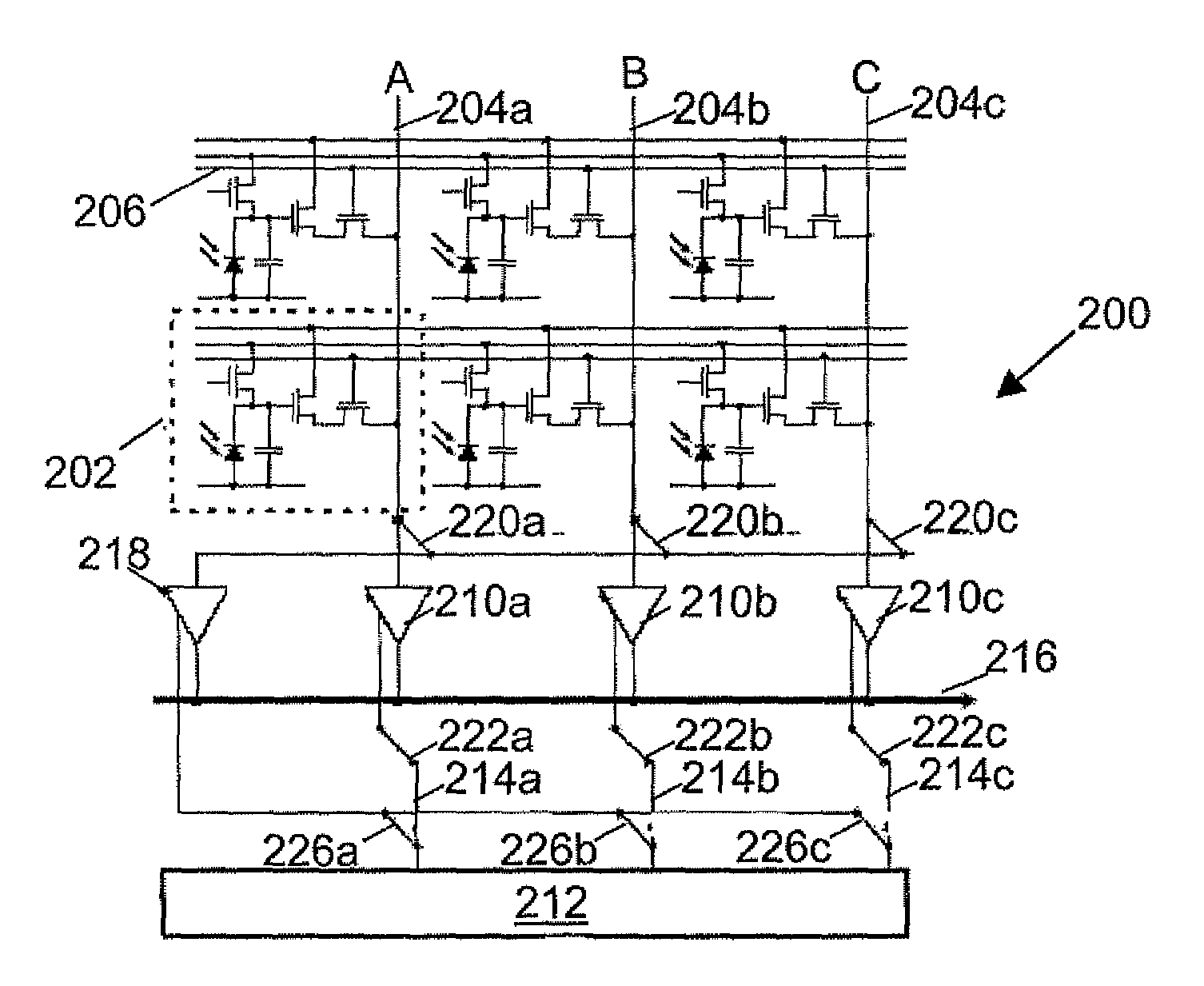
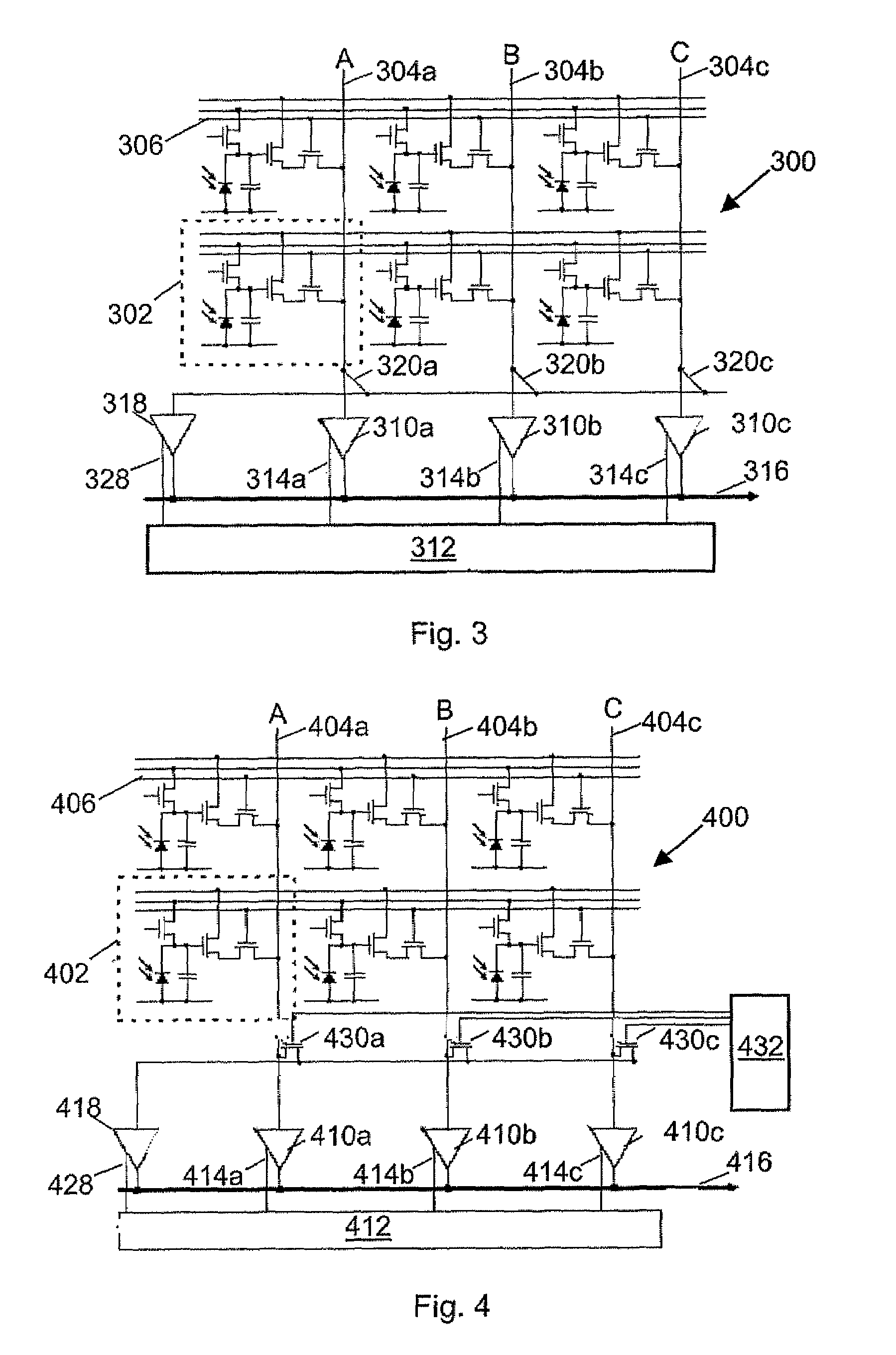
[0020]Typically, two types of issues cause pixel column faults: problems connecting pixels in the readout (“bitline”); and defective column readout. “Column readout” is used as a generic term to describe pixel readout circuitry, which is usually on a per column basis. The column readout may be a simple voltage or charge amplifier; with modern technology, it usually incorporates an analog-digital converter (ADC). The column readout usually also has other processing, such as CDS (correlated double sampling) or other fixed-pattern noise or offset reduction methods. In the context of this invention, “column readout” includes any circuitry connected to a column bitline for reading pixel values.

[0021]With prior-art sensors, if there is a defective column readout circuit, either the whole sensor is declared defective, or the system forced to use some digital correction, which is never 100% transparent and requires post-processing. Post-processing requires additional circuitry, which ultima...


PUM


Abstract

The image sensor has a plurality of pixels arranged in rows and columns to form a pixel array, each pixel column having a column bitline. The image sensor includes a column readout for each column bitline and at least one additional column readout. The additional column readout may be selectively connected to one of the column bitlines. In one embodiment, a defective column readout can be isolated and the additional column readout used as a replacement.

Description

FIELD OF THE INVENTION[0001]The present invention relates to the field of image sensing, and particularly to an image sensor with readout amplifier redundancy.BACKGROUND OF THE INVENTION[0002]There is an increasing tendency for larger number of pixels on image sensors used in devices such as digital still cameras, mobile phone cameras and optical pointing devices, for example. Consequently, sensors have either increased in size or pixels have been manufactured smaller, or often both. The use of finer geometry technologies increase the chance of defects occurring. Typically, the defectivity of an image sensor is proportional to the area.[0003]Defects are caused during manufacture and are usually caused by dust particles obstructing the photolithography process. Resulting defects may be open circuit or short circuit connections. If a defect occurs within a pixel during manufacture, a defective pixel is usually the result. The defective pixel can be either ignored by the user or, if th...

Claims


Application Information

Patent Timeline
Patent Type & Authority Patents(United States)
IPC IPC(8): H01L27/00H03F3/08H04N5/335
CPCH01L27/14603H01L27/14609H01L27/14643H04N5/335H04N25/00H04N25/68
Inventor RAYNOR, JEFFREY
Owner STMICROELECTRONICS (RES & DEV) LTD
Features
  • R&D
  • Intellectual Property
  • Life Sciences
  • Materials
  • Tech Scout
  • Unparalleled Data Quality
  • Higher Quality Content
  • 60% Fewer Hallucinations
Learn More