Transmission line to waveguide interconnect and method of forming same including a heat spreader

a technology of waveguide interconnect and heat spreader, which is applied in the direction of waveguide type devices, optical elements, instruments, etc., can solve the problems of limiting the performance of mcm, difficult manufacturing and assembly, and contributing significantly to transmission losses

Active Publication Date: 2009-01-20
NORTHROP GRUMMAN SYST CORP
View PDF10 Cites 197 Cited by
  • Summary
  • Abstract
  • Description
  • Claims
  • Application Information

AI Technical Summary

Problems solved by technology

These connections, however, may be difficult to manufacture and assemble and often limit the performance of the MCM.
The inductive reactance presented by ribbon 106 is significant at millimeter wave (MMW) frequencies and contributes significantly to transmission losses.
The need to tune out this reactance with printed capacitive elements and the variability of the length of ribbon 106 due to manufacturing constraints results in narrow band performance with unacceptable test yields for many MMW module applications.

Method used


Image

  • Transmission line to waveguide interconnect and method of forming same including a heat spreader
  • Transmission line to waveguide interconnect and method of forming same including a heat spreader
  • Transmission line to waveguide interconnect and method of forming same including a heat spreader

Examples


Embodiment Construction

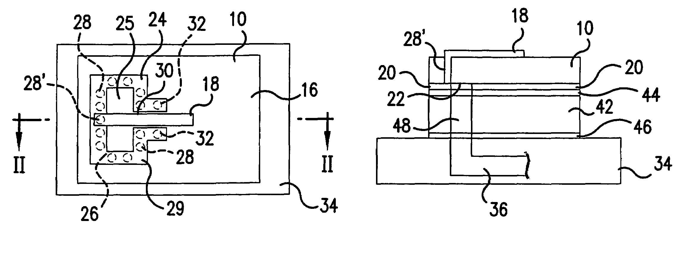
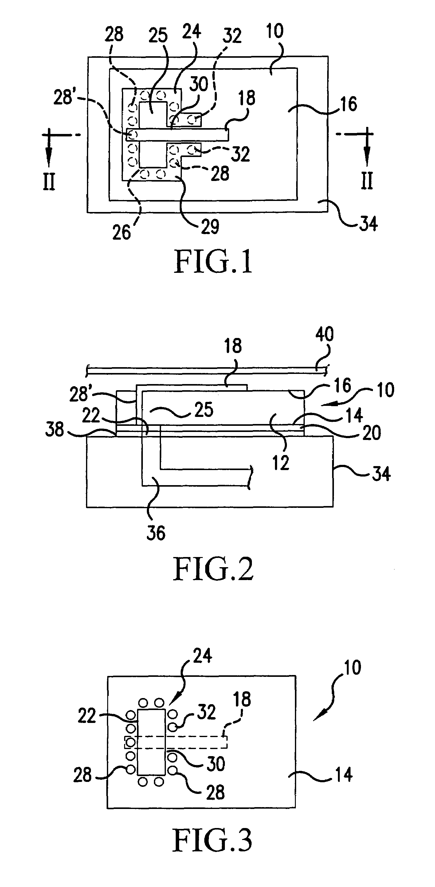
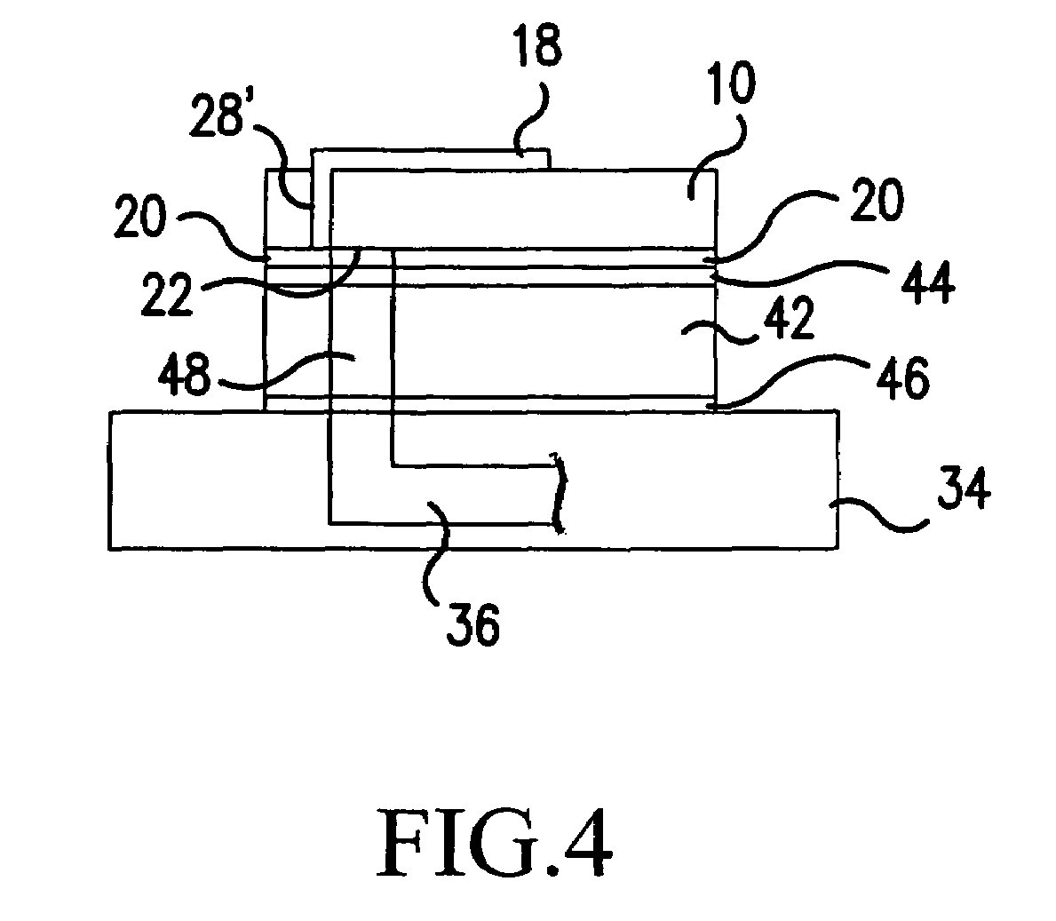
[0019]Referring now to the drawings, wherein the showings are for purposes of illustrating preferred embodiments of the invention only, and not for the purpose of limiting same, and wherein the figures are not drawn to scale, FIGS. 1-3 illustrate a chip 10, which may comprise, for example, a gallium arsenide chip, that includes a dielectric substrate 12 (e.g., FIG. 2) having a first side 14 (e.g., FIGS. 2, 3) and a second side 16 (e.g., FIGS. 1, 2 ) . A transmission line 18 is formed on second side 16, which transmission line in the present embodiment comprises a microstrip trace. A conductive layer of material 20 (e.g., FIG. 2) formed on first side 14 of substrate 12 serves as a ground plane. Signals propagate along transmission line 18 in a well-known manner.

[0020]An opening 22 (e.g., FIGS. 2, 3) having a periphery 24 (e.g. FIGS. 1, 3) is formed in conductive layer 20. A waveguide 25 (FIGS. 1,2) having a waveguide opening 26 (FIG. 1) on second side 16 is defined by a projection of...


PUM


Abstract

An MMIC chip is disclosed that includes a planar substrate having a first surface and a second surface, a conductive layer having an opening on the first surface, a transmission line on the second surface, at least one conductor extending from the conductive layer to the second surface defining a waveguide around the opening, wherein the transmission line is connected to the at least one conductor such that a signal traveling along the transmission line is guided toward the opening in the first side by the at least one conductor.

Description

FIELD OF THE INVENTION[0001]The present invention is directed toward an improved interconnect structure between a transmission line and a waveguide and a method for forming such an interconnect, and, more specifically, toward such an interconnect structure having a low reactive impedance at millimeter and microwave frequencies.BACKGROUND OF THE INVENTION[0002]Multichip modules (MCM) generally comprises a substrate, which may be, for example, a low temperature cofired ceramic (LTCC) material, and one or more chips, such as millimeter / microwave integrated circuits (MMIC), associated therewith. Connections must be provided between the chips and the substrate. These connections, however, may be difficult to manufacture and assemble and often limit the performance of the MCM.[0003]An example of a conventional MCM is illustrated in FIGS. 8-10, wherein a gallium arsenide chip 102 is shown mounted adjacent a multilayer LTCC module 104. A ribbon or wire 106 extends between chip 102 and modul...

Claims


Application Information

Patent Timeline
Patent Type & Authority Patents(United States)
IPC IPC(8): H01P5/107
CPCH01P5/107
Inventor STENGER, PETER A.
Owner NORTHROP GRUMMAN SYST CORP
Why Eureka
Try Eureka