Radiation tolerant solid-state relay

a solid-state relay, radiation-tolerant technology, applied in the direction of electrical equipment, electronic switching, pulse technique, etc., can solve the problems of large variation in current from the source to the drain, limited sources of supply, and the effect of large gate voltage signal, high radiation dose, and large signal magnitud

Inactive Publication Date: 2009-02-24
SUMMER STEVEN E
View PDF7 Cites 4 Cited by
  • Summary
  • Abstract
  • Description
  • Claims
  • Application Information

AI Technical Summary

Benefits of technology

[0014]The object of this invention is to implement radiation hardened solid state relay circuits, having controlled and stable rise and fall times, using non-radiation hardened transistors. This invention is a method of producing an economical solid state relay circuit or switching circuit that can operate in a high ionizing radiation dose environment such as found in spacecraft and particle accelerator applications.
[0016]Another object of the present invention is to provide a P-FET Drive with certain requirements for operating in radiation environments. For instance, in the on state, negative gate to source drive waveform must be sufficiently high in magnitude to saturate the drain to source channel. It must, however, not be so high that the gate to source breakdown voltage rating of the FET is exceeded. It is important to maximize the magnitude of the gate voltage signal, because the higher the signal magnitude is, the higher radiation dose the FET will tolerate and still work acceptably in the circuit. In the off state gate to source drive signal must be sufficiently low to reduce current flow through the drain to source channel. It must, however, not be so high in positive magnitude that that the gate can rupture due to passage of high energy particles normally encountered in radiation environments.

Problems solved by technology

A small change in gate voltage can cause a large variation in current from the source to the drain.
In these specific applications, the solid state relays are subjected to many forms of radiation damage by the surrounding environment.
However, these parts have limited sources of supply, are expensive and may have long lead times, leading to higher prices and longer delivery times for the radiation tolerant circuits that incorporate these types of parts.
Normally, the performance of non-radiation hardened FETs when exposed to radiation, if conventional non-radiation hardened N Channels FETs are used, in switching applications where radiation is present, the function tends to fail at relatively low radiation levels because the gate threshold voltage of the N channel FET shifts more negatively with accumulated radiation dose, and ultimately falls close to zero.
Therefore, the part is difficult to control.

Method used


Image

  • Radiation tolerant solid-state relay
  • Radiation tolerant solid-state relay
  • Radiation tolerant solid-state relay

Examples


Embodiment Construction

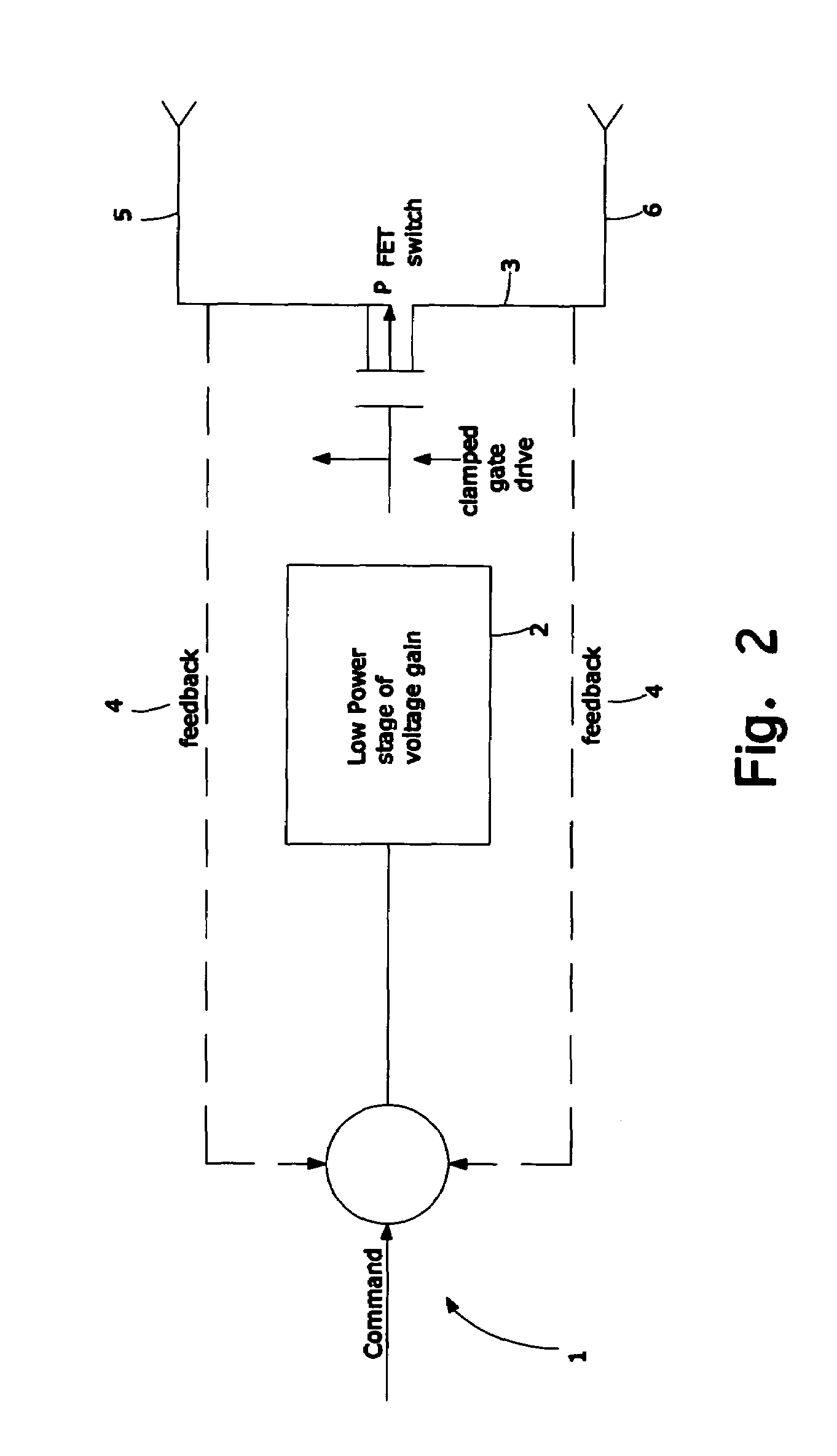
[0019]In accordance with a preferred embodiment of the present invention, the gate drive signal should be high enough to saturate the drain to source channel. It should not, however, be so high that the gate to source breakdown voltage rating of the FET is exceeded. Preferably, the FET operates close to its maximum gate voltage signal. Higher signals can handle higher radiation levels, allowing the FET to function across a larger range of radiation exposure.

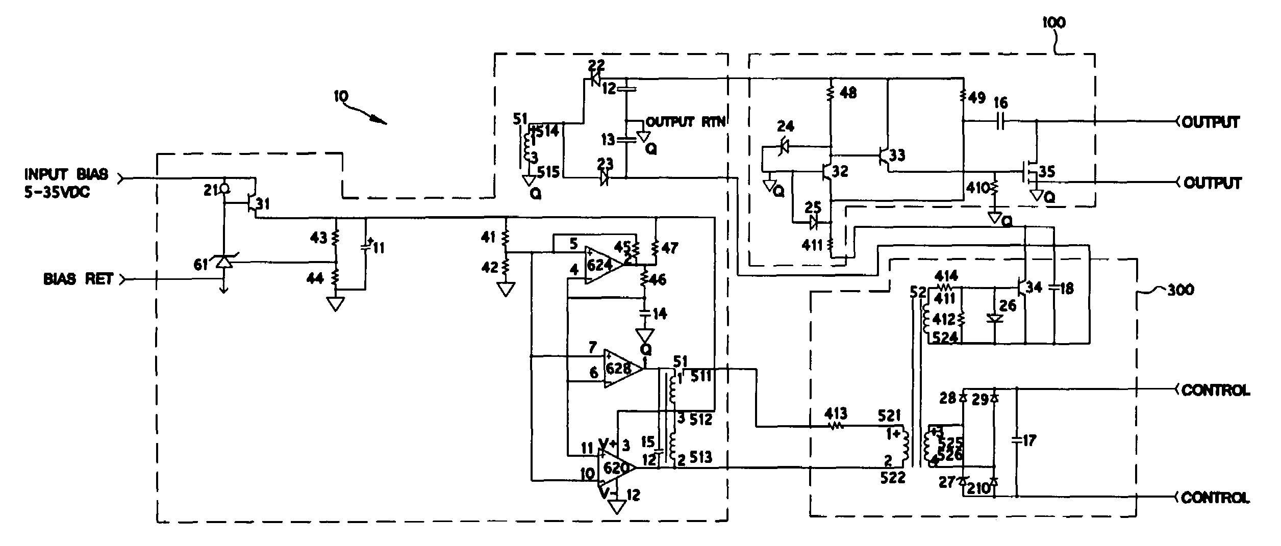
[0020]FIG. 1 is a schematic diagram of a radiation-tolerant solid-state relay generally indicated by reference numeral 10 in accordance with a preferred embodiment of the present invention. This circuit example operates from a voltage source 102 to 50 VDC, but nominally 28 VDC. It may, however, be readily scaled for different bus voltages.

[0021]The circuit 10 includes three galvanically isolated sections, the bias section 200, the control section 300 and the power switching section 100.

[0022]The bias section 200 provides transfor...


PUM


Abstract

The present invention provides a radiation-tolerant, solid-state-relay without radiation-hardened parts. In further detail, the solid-state-relay includes a non-hardened P-channel MOSFET, a low power storage of voltage gain and a feedback signal with the low power stage of voltage gain being relatively insensitive to radiation effects.

Description

CROSS-REFERENCE TO RELATED APPLICATIONS[0001]This application is a continuation-in-part of application Ser. No. 10 / 963,957, filed Oct. 12, 2004, now U.S. Pat. No. 7,132,877.FIELD OF THE INVENTION[0002]The present invention deals with electrical components and more specifically, a radiation-tolerant solid-state relay without radiation-hardened parts.BACKGROUND OF THE INVENTION[0003]Solid-state relays perform functions similar to electromagnetic relays, but are more reliable, since there are no moving parts. Since the turn on and turn off times of a solid-state relay are controllable, the solid-state relay also minimizes the generation of switching transients.[0004]A preferred semiconductor device for power control in a solid-state relay is the insulated gate FET (Field Effect Transistor) because of its high power gain. FETs used for power switching use are usually enhancement mode types. This means that they are normally non-conducting. When a gate voltage above a threshold is applie...

Claims


Application Information

Patent Timeline
Patent Type & Authority Patents(United States)
IPC IPC(8): H03K17/687
CPCH03K17/691
Inventor SUMMER, STEVEN E.
Owner SUMMER STEVEN E
Why Eureka
Try Eureka