Radiation tolerant electrical component with non-radiation hardened FET

a technology of radiation hardening and electrical components, applied in the direction of dc-dc conversion, power conversion systems, instruments, etc., can solve the problems of large variation in current from the source to the drain, uncontrollable fet, and designed radiation hardening n channel fet, etc., to maximize the magnitude of gate voltage signal and signal magnitude. , the effect of high magnitud

Active Publication Date: 2012-02-28
MODULAR DEVICES
View PDF17 Cites 0 Cited by
  • Summary
  • Abstract
  • Description
  • Claims
  • Application Information

AI Technical Summary

Benefits of technology

[0016]Accordingly, in the on state for the P-channel FET, a negative gate to source drive waveform, sufficiently high in magnitude, saturates the drain to source channel. It must not be so high however, that the gate to source breakdown voltage rating of the FET is exceeded. It is important to maximize the magnitude of the gate voltage signal, because the higher the signal magnitude is, the higher radiation dose the FET will tolerate and still work acceptably in the DC / DC converter circuit.

Problems solved by technology

A small change in gate voltage can cause a large variation in current from the source to the drain.
In other words, the FET is uncontrollable because the current running through the channel cannot be easily shut off.
Additionally, the downside of these specially designed radiation hardened N channel FETs is that they (1) have a sole source of supply, (2) are expensive, (3) have long lead times and (4) have limited availability.
In turn, this affects the market for radiation tolerant DC / DC converter circuits incorporating this type of FET with higher prices, longer delivery times and limited availability.

Method used


Image

  • Radiation tolerant electrical component with non-radiation hardened FET
  • Radiation tolerant electrical component with non-radiation hardened FET
  • Radiation tolerant electrical component with non-radiation hardened FET

Examples


Embodiment Construction

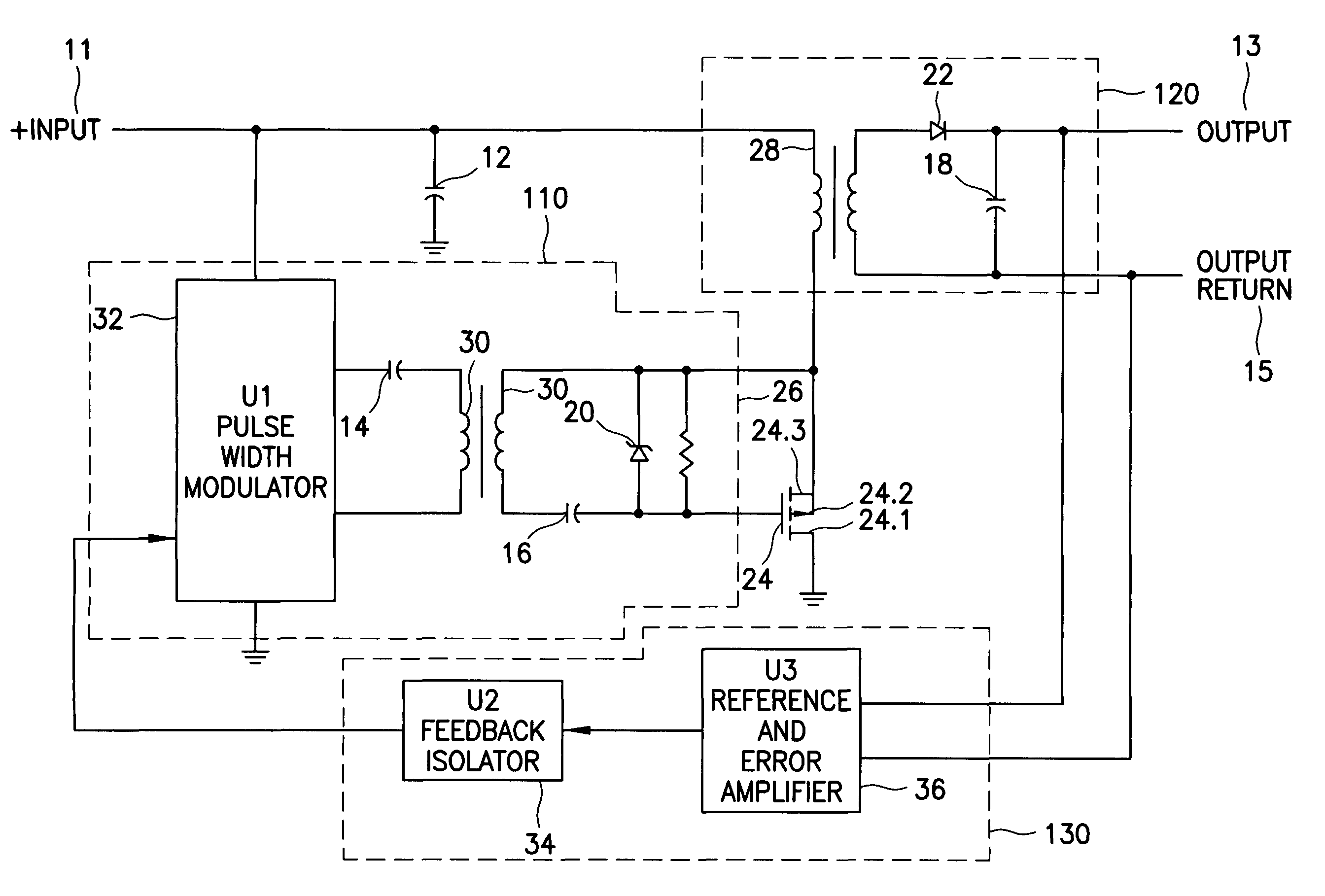
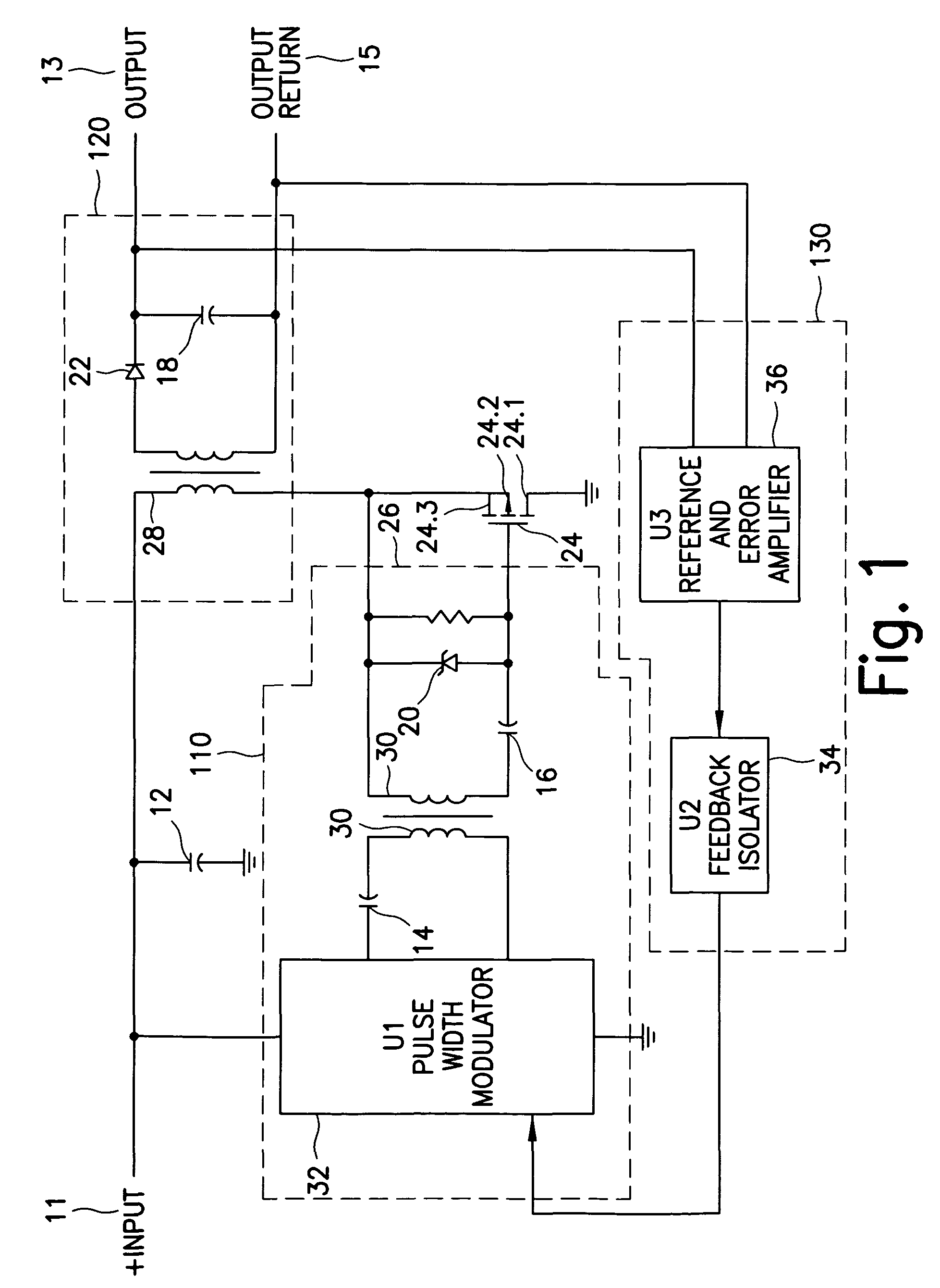
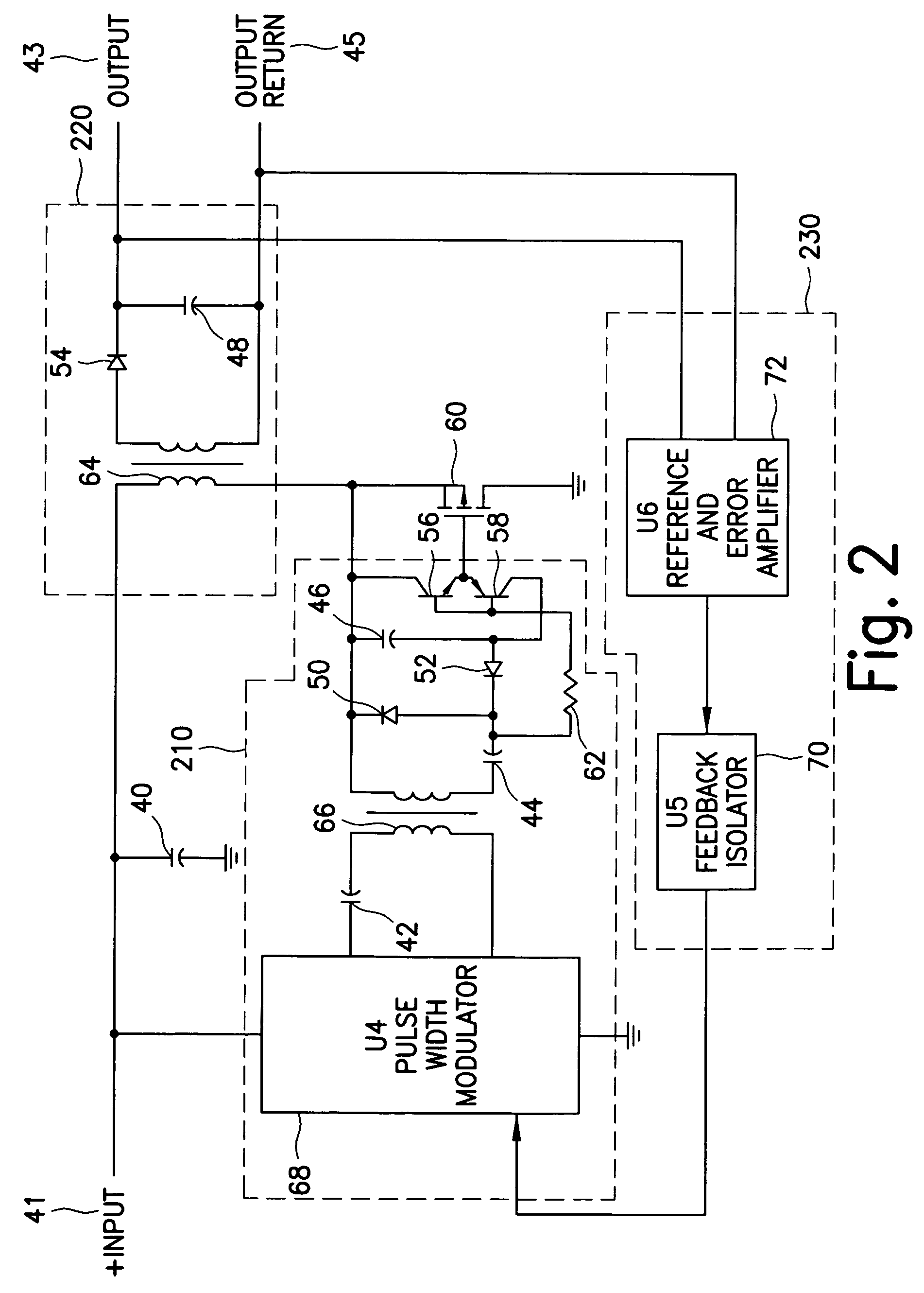
[0021]Field-effect transistors exist in two major classifications, the junction FET (JFET) and the metal-oxide-semiconductor FET (MOSFET). A MOSFET is a special type of FET that works by electronically varying the width of a channel along which charge carriers (electrons or holes) flow. Wider channels provide better conductivity. The charge carriers enter the channel at the source, and exit via the drain. The width of the channel is controlled by the voltage on an electrode called the gate, which is located physically between the source and the drain and is insulated from the channel by an extremely thin layer of metal oxide.

[0022]There are two ways in which a MOSFET can function. The first is known as depletion mode. When there is no voltage on the gate, the channel exhibits its maximum conductance. As the voltage on the gate increases (either positively or negatively, depending on whether the channel is made of P-type or N-type semiconductor material), the channel conductivity dec...


PUM


Abstract

A radiation tolerant electrical component is provided without a radiation hardened material FET. A p-channel MOSFET provides switching capabilities in radiated environments because its gate voltage starts at a negative value and becomes more negative with exposure to radiation. Therefore, the gate is still controllable when exposed to radiation.

Description

CROSS-REFERENCE TO RELATED APPLICATION[0001]This application is a continuation-in-part of co-pending application Ser. No. 11 / 288,653 filed Nov. 29, 2005, which, in turn, is a continuation of application Ser. No. 10 / 806,872 filed Mar. 22, 2004, now U.S. Pat. No. 6,982,883.FIELD THE INVENTION[0002]The object of this invention is a method of producing an economical DC / DC converter or switching regulator that can operate in a high ionizing radiation dose and high energy particle environments, such as found in space and particle accelerator applications.BACKGROUND OF THE INVENTION[0003]DC / DC converters are electronic devices that use switching components, such as field effect transistors (FETs) to transform voltage from one level to another. Typically, the output voltage is regulated and protected against short circuits. In many cases, the input and output potentials are galvanically isolated from each other.[0004]A preferred semiconductor device for power switching in a DC / DC converter ...

Claims


Application Information

Patent Timeline
Patent Type & Authority Patents(United States)
IPC IPC(8): H02M3/335H02H7/122
CPCH02M3/28H02M3/33523
Inventor SUMMER, STEVEN E.
Owner MODULAR DEVICES
Why Eureka
Try Eureka