Magnetoresistive device and magnetic memory using the same
a magnetic memory and magnetoresistance technology, applied in the field of magnetoresistance devices and magnetic memory using the same, can solve the problems of reducing the writing margin, erroneous writing operation of toggle-writing-based mram, and inevitably facing limit of the effort to reduce the write current, so as to reduce the magnetic field and reduce the write current. , the effect of increasing the writing margin
- Summary
- Abstract
- Description
- Claims
- Application Information
AI Technical Summary
Benefits of technology
Problems solved by technology
Method used
Image
Examples
first embodiment
2. First Embodiment
[0123]FIG. 15A is a sectional view illustrating an exemplary structure of a memory cell of an MRAM in a first embodiment of the present invention. The MRAM is provided with a substrate 1, a lower electrode layer 2 formed on the substrate 1, an antiferromagnetic layer 3 formed of antiferromagnetic material, a fixed magnetic layer 4, a non-magnetic layer 5, a free magnetic layer 6, and a contact electrode layer 7. The antiferromagnetic layer 3 exerts exchange interaction on the fixed magnetic layer 4 to fix the magnetization of the fixed magnetic layer 4. The fixed magnetic layer 4 is composed of an SAF including of a ferromagnetic layer 41, an AF (antiferromagnetically) coupling non-magnetic layer 42 and a ferromagnetic layer 43. The magnetizations of the fixed magnetic layer 4 are fixed by the antiferromagnetic layer 3. In an alternative embodiment, the fixed magnetic layer 4 may be formed of a single ferromagnetic layer.
[0124]The non-magnetic layer 5 is formed of...
second embodiment
3. Second Embodiment
[0142]FIG. 16A is a sectional view illustrating an exemplary structure of a memory cell of an MRAM in a second embodiment of the present invention. In this embodiment, the free magnetic layer 6 within the MRAM cell is designed differently from the free magnetic layer 6 presented in the first embodiment.
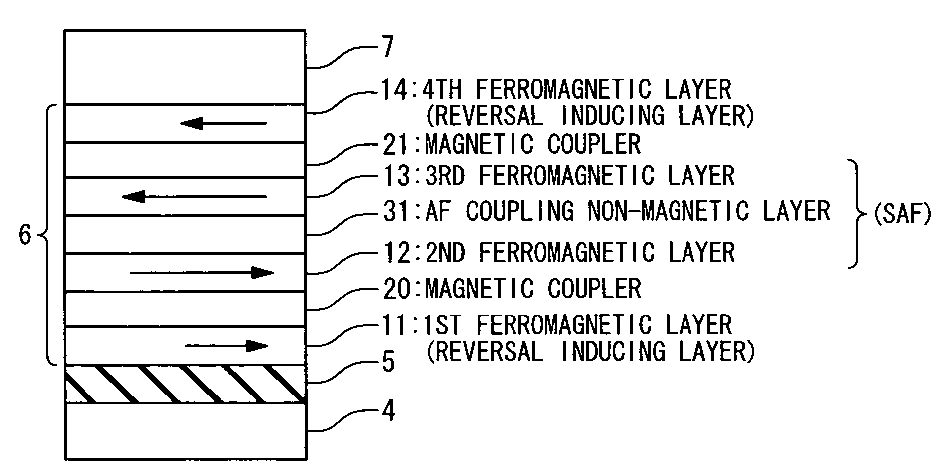
[0143]Differently from the MRAM in the first embodiment which includes two magnetic couplers and two reversal inducing layers, the MRAM in the second embodiment incorporates one magnetic coupler and one reversal inducing layer within the free magnetic layer 6 is provided with. More specifically, the free magnetic layer 6 is provided with a second ferromagnetic layer 12 formed on the non-magnetic layer 5, a non-magnetic layer 31 formed thereon, a third ferromagnetic layer 13 formed on the non-magnetic layer 31, a fourth ferromagnetic layer 14, and a magnetic coupler 21 interposed between the third and fourth ferromagnetic layers 13 and 14. The contact electrode laye...
third embodiment
4. Third Embodiment
[0147]In a third embodiment, the free ferromagnetic layer 6 incorporates a multilayer SAF composed of three or more ferromagnetic layers, adjacent two of which are antiferromagnetically coupled. The use of the multilayer SAF does not deteriorate the reversal inducing effect of the present invention. FIGS. 18A and 18B illustrate exemplary structures in the third embodiment.
[0148]An MRAM shown in FIG. 18A is provided with a free magnetic layer 6 incorporating an SAF composed of three ferromagnetic layers and a reversal inducing layer. The structure of the MRAM shown in FIG. 18A is identical to that described in the first embodiment, except for the structure of the free magnetic layer 6. In the MRAM shown in FIG. 18A, a ferromagnetic layer 60 is provided on the non-magnetic layer 5. Additionally, a multilayer stack composed of an AF coupling non-magnetic layer 31, a ferromagnetic layer 61, an AF coupling non-magnetic layer 32, and a ferromagnetic layer 62 is formed o...
PUM
 Abstract
Description
Claims
Application Information


