Magnetoresistive device and magnetic memory using the same

a magnetic memory and magnetoresistance technology, applied in the field of magnetoresistance devices and magnetic memory using the same, can solve the problems of reducing the writing margin, erroneous writing operation of toggle-writing-based mram, and inevitably facing limit of the effort to reduce the write current, so as to reduce the magnetic field and reduce the write current. , the effect of increasing the writing margin

Active Publication Date: 2006-11-23
NEC CORP
View PDF14 Cites 90 Cited by
  • Summary
  • Abstract
  • Description
  • Claims
  • Application Information

AI Technical Summary

Benefits of technology

[0022] Therefore, an object of the present invention is to provide a novel technique for reducing a magnetic field necessary for data writing with an increased writing margin in a toggle-writing based MRAM, and to thereby achieve the reduction in a write current and the suppression of unsuccessful data writing.
[0023] Another object of the present invention to provide a novel technique for reducing a magnetic field necessary for data writing with stable antiferromagnetic coupling in an MRAM using free magnetic layers incorporating SAFs having reduced net magnetizations. This effectively reduces the write current of the MRAM, and avoids unsuccessful data writing.
[0025] In the magnetoresistive element thus structured, the first reversal inducing layer, which has the relatively reduced coercive field, effectively enhances the magnetization reversal of the ferromagnetic layers within the first synthetic antiferromagnet, and thereby reduces the magnetic field necessary for data writing.
[0035] In order to improve thermal stability of the free magnetic layer, the magnetic coupler preferably includes oxide of element that has an oxide formation energy lower than that of magnetic element included in the ferromagnetic layers contacted with the top and bottom surface of the magnetic coupler. It is also preferable that the magnetic coupler includes nitride of element that has a nitride formation energy lower than that of magnetic element included in the ferromagnetic layers contacted with the top and bottom surface of the magnetic coupler. Instead, it is also preferable that the magnetic coupler includes carbide of element that has a carbide formation energy lower than that of magnetic element included in the ferromagnetic layers contacted with the top and bottom surface of the magnetic coupler. The magnetic coupler such-designed may include a material selected from a group consisting of magnesium, aluminum, silicon, germanium, lithium, beryllium, barium, calcium, titanium, vanadium, chromium, manganese, zirconium, hafnium, tantalum, niobium, molybdenum, cerium, yttrium, and lanthanum. In order to control magnetic characteristics and to improve thermal stability in the magnetoresistance ratio, the magnetoresistive element is preferable designed so that one face of the first reversal inducing layer is directly connected with the non-magnetic layer between the free and fixed magnetic layers, and another face is directly connected with the magnetic coupler thus designed, that the magnetic coupler being directly connected with one ferromagnetic layer within the synthetic antiferromagnet, the one ferromagnetic layer incorporating a film including non-magnetic element. The film including non-magnetic element provides control of the strength of the antiferromagnetic coupling within the first synthetic antiferromagnet.

Problems solved by technology

This is however, accompanied by a problem that the writing margin is also reduced.
Therefore, the reduction in the spin-flop field Hflop undesirably causes erroneous write operation of the toggle-writing-based MRAM.
Therefore, an effort for reducing the write currents inevitably faces limit in a conventional toggle-writing-based MRAM.
However, the disclosed SAF structure does not address maintaining or improving the saturation field of the SAF.

Method used


Image

  • Magnetoresistive device and magnetic memory using the same
  • Magnetoresistive device and magnetic memory using the same
  • Magnetoresistive device and magnetic memory using the same

Examples


first embodiment

2. First Embodiment

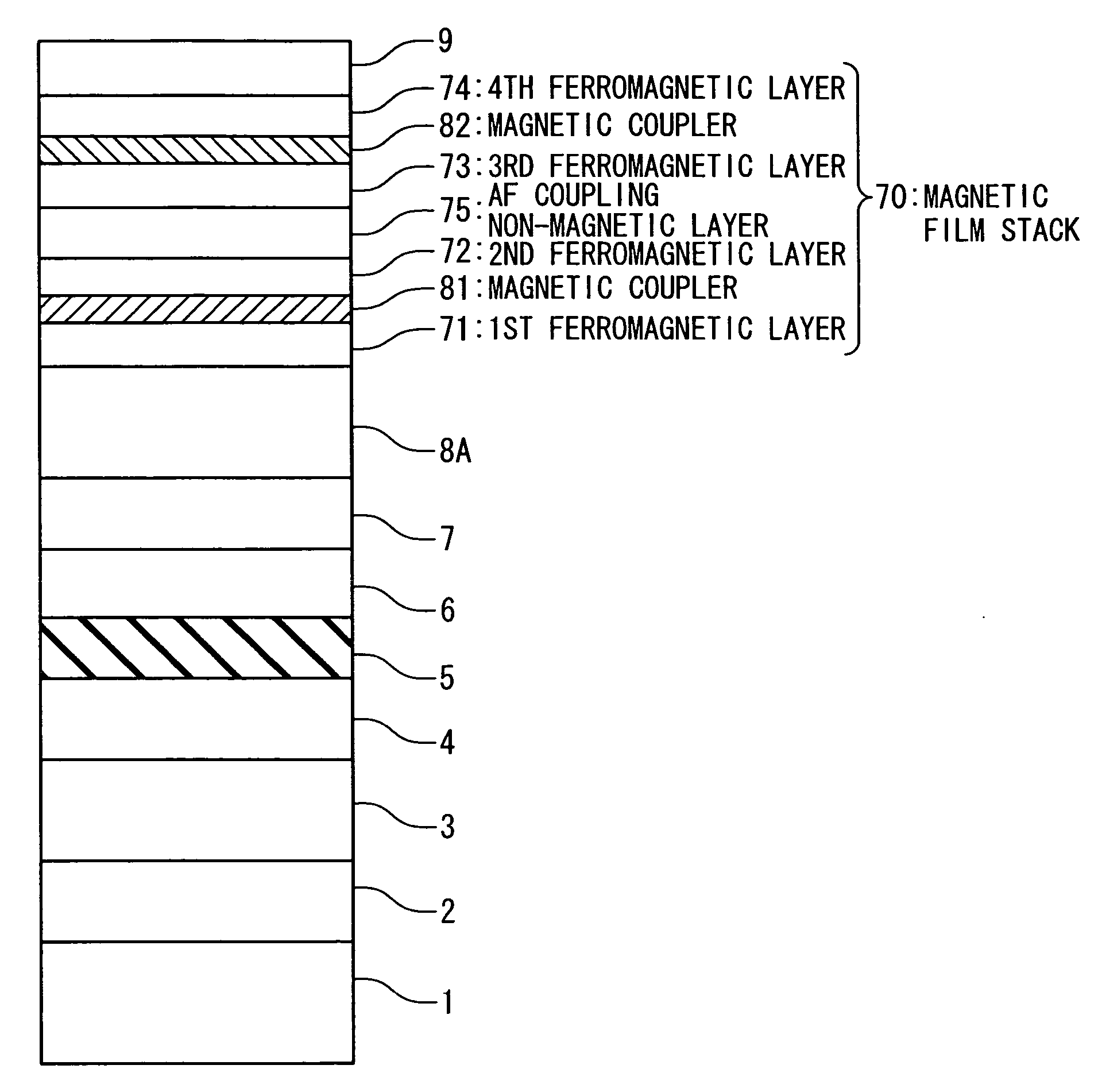
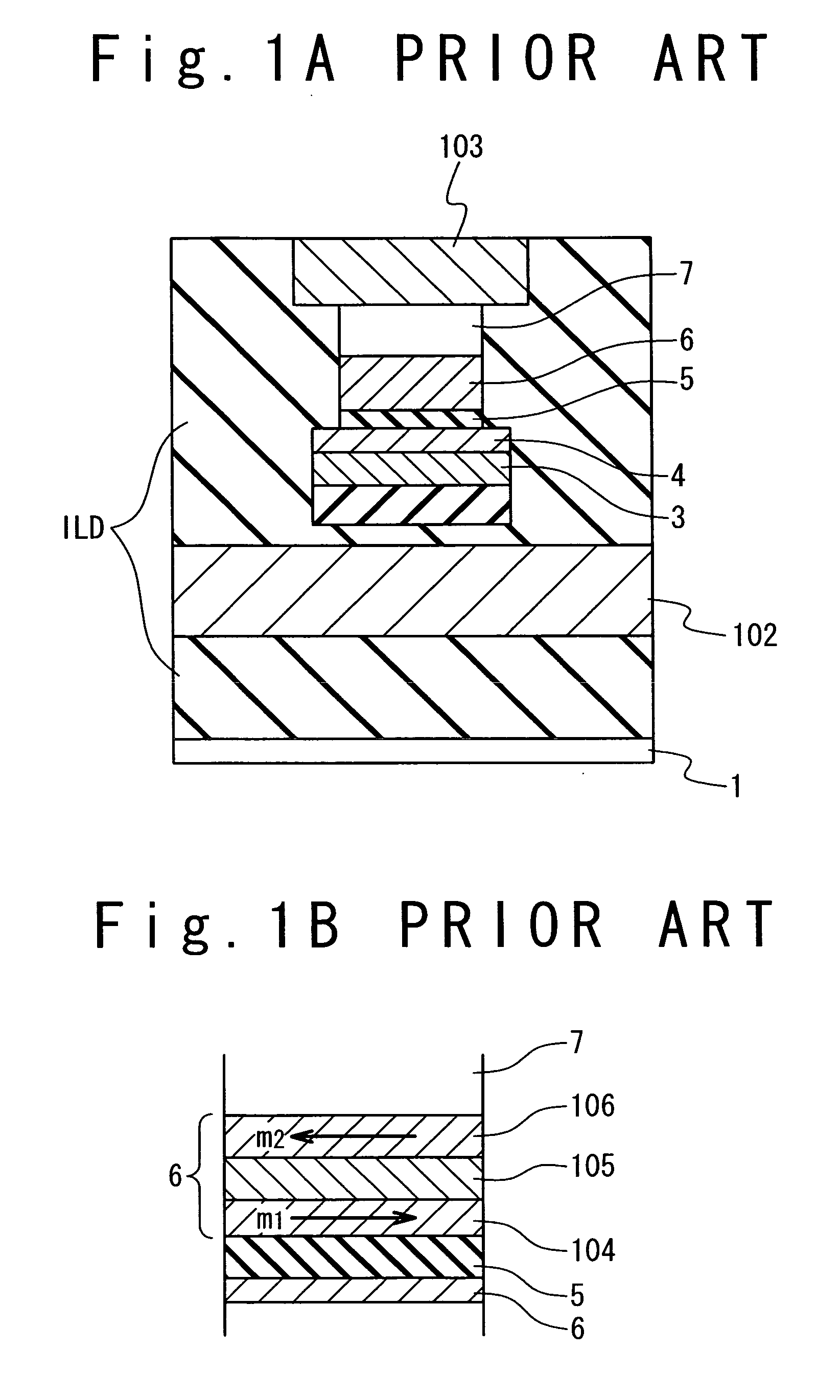
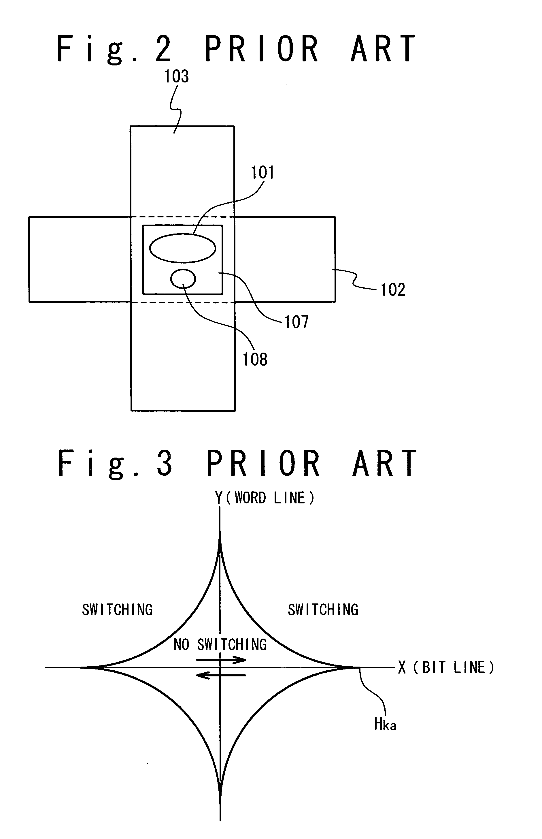
[0120]FIG. 15A is a sectional view illustrating an exemplary structure of a memory cell of an MRAM in a first embodiment of the present invention. The MRAM is provided with a substrate 1, a lower electrode layer 2 formed on the substrate 1, an antiferromagnetic layer 3 formed of antiferromagnetic material, a fixed magnetic layer 4, a non-magnetic layer 5, a free magnetic layer 6, and a contact electrode layer 7. The antiferromagnetic layer 3 exerts exchange interaction on the fixed magnetic layer 4 to fix the magnetization of the fixed magnetic layer 4. The fixed magnetic layer 4 is composed of an SAF including of a ferromagnetic layer 41, an AF (antiferromagnetically) coupling non-magnetic layer 42 and a ferromagnetic layer 43. The magnetizations of the fixed magnetic layer 4 are fixed by the antiferromagnetic layer 3. In an alternative embodiment, the fixed magnetic layer 4 may be formed of a single ferromagnetic layer.

[0121] The non-magnetic layer 5 is formed ...

second embodiment

3. Second Embodiment

[0139]FIG. 16A is a sectional view illustrating an exemplary structure of a memory cell of an MRAM in a second embodiment of the present invention. In this embodiment, the free magnetic layer 6 within the MRAM cell is designed differently from the free magnetic layer 6 presented in the first embodiment.

[0140] Differently from the MRAM in the first embodiment which includes two magnetic couplers and two reversal inducing layers, the MRAM in the second embodiment incorporates one magnetic coupler and one reversal inducing layer within the free magnetic layer 6 is provided with. More specifically, the free magnetic layer 6 is provided with a second ferromagnetic layer 12 formed on the non-magnetic layer 5, a non-magnetic layer 31 formed thereon, a third ferromagnetic layer 13 formed on the non-magnetic layer 31, a fourth ferromagnetic layer 14, and a magnetic coupler 21 interposed between the third and fourth ferromagnetic layers 13 and 14. The contact electrode la...

third embodiment

4. Third Embodiment

[0144] In a third embodiment, the free ferromagnetic layer 6 incorporates a multilayer SAF composed of three or more ferromagnetic layers, adjacent two of which are antiferromagnetically coupled. The use of the multilayer SAF does not deteriorate the reversal inducing effect of the present invention. FIGS. 18A and 18B illustrate exemplary structures in the third embodiment.

[0145] An MRAM shown in FIG. 18A is provided with a free magnetic layer 6 incorporating an SAF composed of three ferromagnetic layers and a reversal inducing layer. The structure of the MRAM shown in FIG. 18A is identical to that described in the first embodiment, except for the structure of the free magnetic layer 6. In the MRAM shown in FIG. 18A, a ferromagnetic layer 60 is provided on the non-magnetic layer 5. Additionally, a multilayer stack composed of an AF coupling non-magnetic layer 31, a ferromagnetic layer 61, an AF coupling non-magnetic layer 32, and a ferromagnetic layer 62 is forme...


PUM


Abstract

A magnetic film stack is composed of a synthetic antiferromagnet including a plurality of ferromagnetic layers, adjacent two of which are antiferromagnetically coupled through a non-magnetic layer; and a reversal inducing layer exhibiting ferromagnetism. The reversal inducing layer is ferromagnetically coupled to the synthetic antiferromagnet, and designed to have a coercive field smaller than a magnetic field at which antiferromagnetic coupling within the synthetic antiferromagnet starts to be decoupled.

Description

BACKGROUND OF THE INVENTION [0001] 1. Field of the Invention [0002] The present invention relates to a magnetoresistance device and a magnetic memory using the same. Particularly, the present invention relates to a magnetoresistance device provided with a free magnetic layer incorporating a plurality of ferromagnetic layers, adjacent two of which are antiparallelly coupled. [0003] 2. Description of the Related Art [0004] In recent yeas, research and develop activity in the field of the MRAM (Magnetic Random Access Memory) has been enhanced, due to the fast write and read access. FIG. 1A illustrates an exemplary structure of a typical MRAM. The MRAM shown in FIG. 1 is composed of a substrate 1, word lines 102 and bit lines 103 (each one shown), and magnetoresistive elements (one shown) each including an antiferromagnetic layer 3, a fixed magnetic layer 4, a non-magnetic layer 5, a free magnetic layer 5. The magnetoresistive elements are arranged at respective intersections of the wor...

Claims


Application Information

Patent Timeline
Patent Type & Authority Applications(United States)
IPC IPC(8): G11C11/00
CPCB82Y25/00H01F10/3272H01F10/3254G11C11/16G11C11/161G11C11/1675H10N50/10H10N50/85G11C11/15H10B61/00
Inventor FUKUMOTO, YOSHIYUKI
Owner NEC CORP
Why Eureka
Try Eureka