Temporary structure to reduce stress and warpage in a flip chip organic package

a technology of flip chip and organic packaging, applied in the field of flip chip packaging, can solve the problems of substrate deformation in the z-direction, compromising yield, warpage, etc., and achieve the effect of reducing the residual stress between the underfill and the ic chip, and reducing the stress and warpag

Inactive Publication Date: 2009-05-26
IBM CORP
View PDF23 Cites 4 Cited by
  • Summary
  • Abstract
  • Description
  • Claims
  • Application Information

AI Technical Summary

Problems solved by technology

This mismatch in CTE imposes large strains on the C4s and / or the underlying circuitry of the IC chip, thereby compromising yield (e.g. failure during temperature excursions such as solder reflow for the C4 interconnections) and reliability (e.g. failure during application temperature excursions).
One drawback of this mitigation approach is that the underfill material, once cured, polymerized, and adhesively bonded to the C4s, IC chip, and substrate, limits the lateral (X-Y) contraction of the substrate during the cool down cycle of underfill cure, thereby causing: (1) the substrate to deform in the Z-direction (warpage); and (2) high residual stresses between the underfill and the IC chip, especially at the IC corners where the Distance to Neutral Point (DNP) (i.e., center point of the IC chip) is highest.
Moreover, if the underfill is not present during initial joining of the IC chip to the substrate, then no such protection is afforded at this stage.
However, drawbacks to these solutions include increased difficulties in affecting the initial C4 joints and compromised reliability attributes.
While providing improved resistance against warpage, such a process increases assembly cost and imparts greater stresses to other interfaces.
Another issue with the aforementioned trends in micro-electronic packaging, and specifically involving higher densities and larger IC chips, is that organic substrates are becoming less co-planar due to increased warping prior to any C4 joining to the IC chip.
However, the greater the amount of warpage, the more difficult it becomes to effect 100% joining efficiency of all C4 interconnections between the IC chip and the substrate.

Method used


Image

  • Temporary structure to reduce stress and warpage in a flip chip organic package
  • Temporary structure to reduce stress and warpage in a flip chip organic package
  • Temporary structure to reduce stress and warpage in a flip chip organic package

Examples


Embodiment Construction

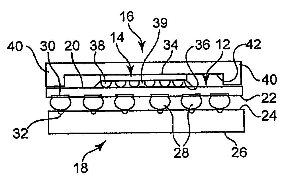
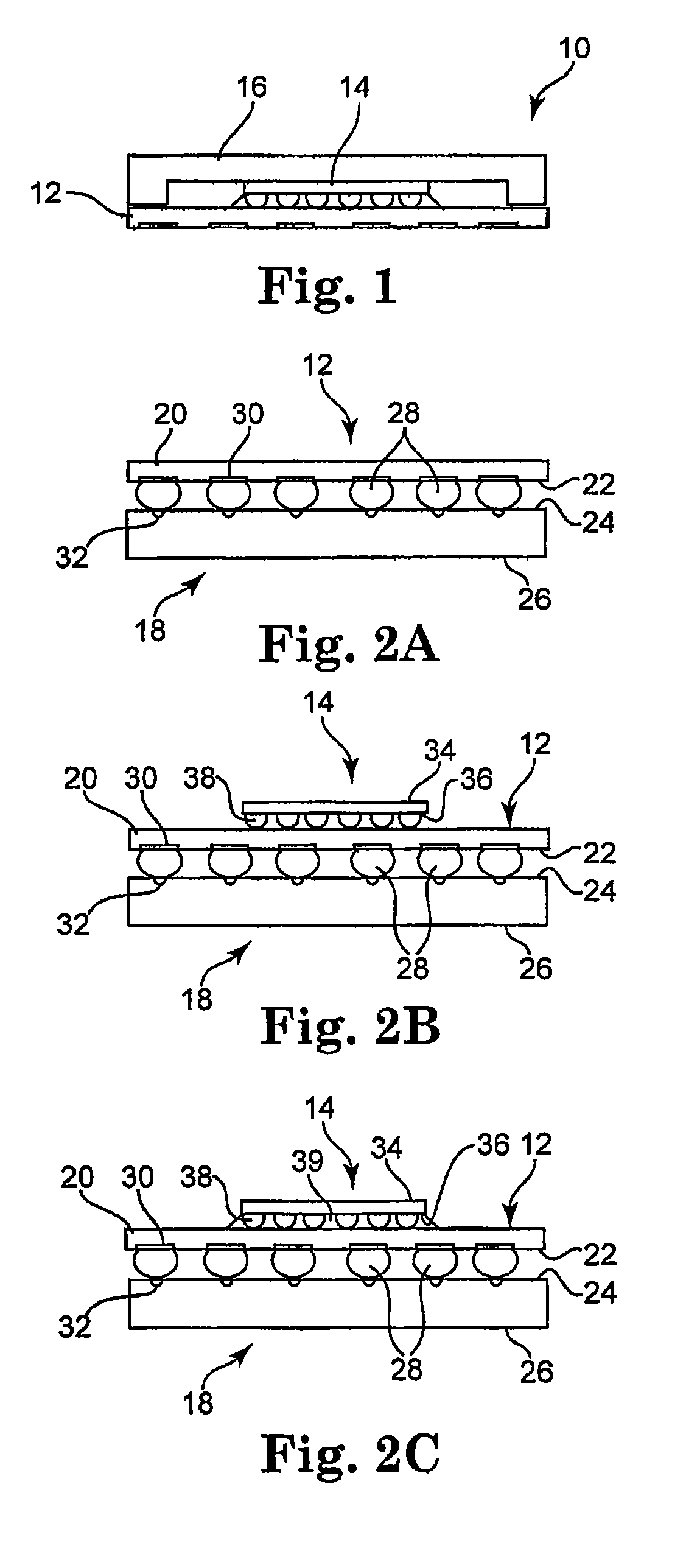
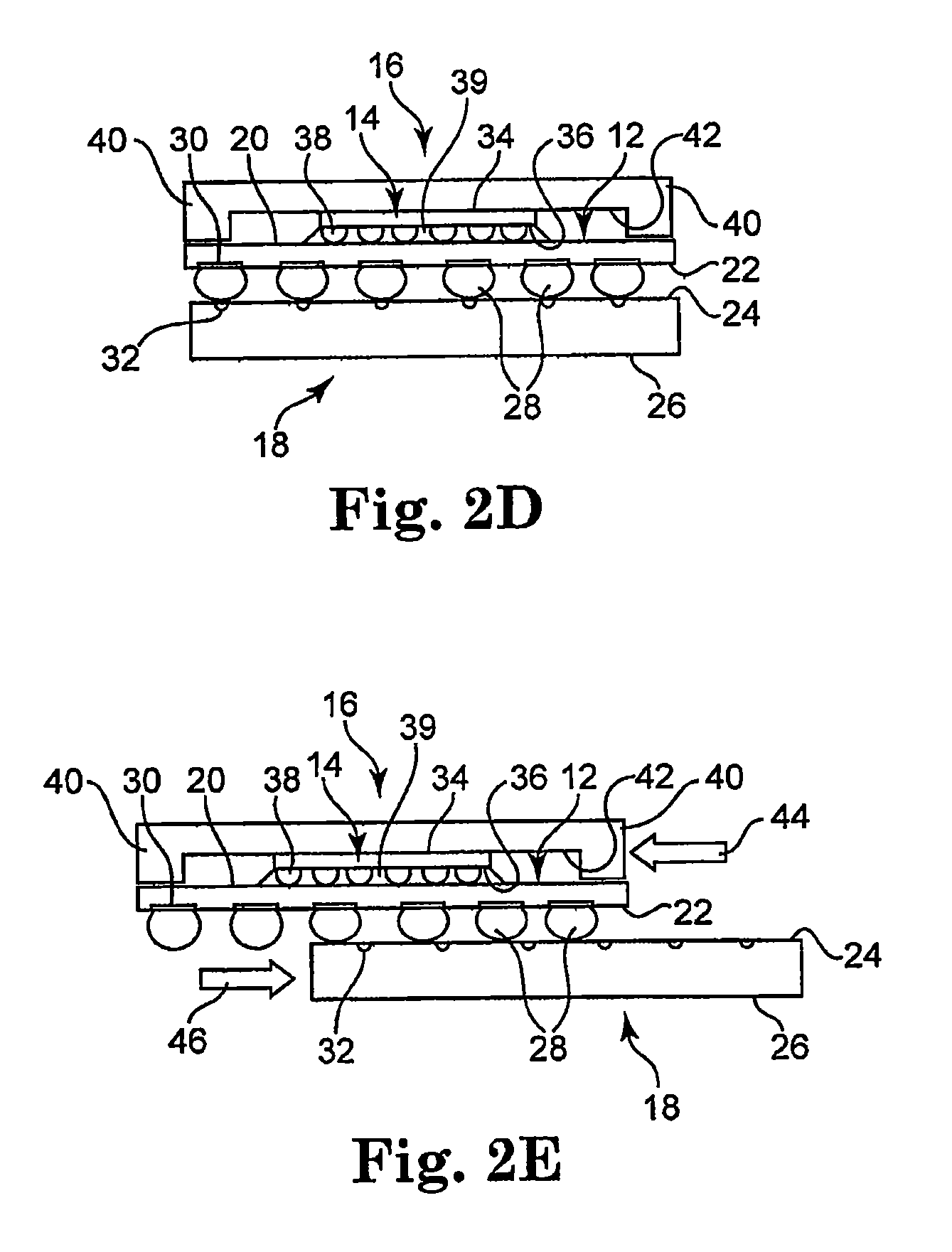
[0011]The present invention will be described in detail with reference to the figures below. However, generally speaking, the present invention is a structure and method for reducing stress and warpage in flip chip packages. The invention includes providing a temporary structure having a CTE similar to that of an IC chip of a flip chip package, bonding the temporary structure to an organic substrate prior to interconnecting the IC chip and organic substrate with C4s, and “de-bonding” the temporary structure from the flip chip package at some stage prior to interconnecting the final flip chip package assembly to its corresponding card, board or other receiving medium. This invention provides numerous benefits, including but not limited to the following: reducing substrate warpage prior to IC chip assembly; reducing stresses imparted to underlying IC chip circuitry during IC chip joining without the need of a pre-applied underfill; reducing package warpage during underfill cure / cool d...


PUM


Abstract

A flip chip assembly having reduced stress and warpage comprises a flip chip package including an organic substrate and an integrated circuit chip, a temporary structure having a coefficient of thermal expansion that is substantially similar to a coefficient of thermal expansion of the integrated circuit chip, and a cap member coupled to a top side of the organic substrate. A bottom side of the integrated circuit chip is bonded to the top side of the organic substrate with controlled chip collapse columns. Additionally, a bottom side of the organic substrate is soldered to a top side of the temporary structure with solder interconnections that are applied to a plurality of solder pads on the top side of the temporary structure, the position of the solder pads on the temporary structure mirroring the position of a plurality of solder pads on the bottom side of the organic substrate.

Description

CROSS REFERENCE TO RELATED APPLICATION(S)[0001]The present application is a continuation application of application Ser. No. 12 / 107,316 filed Apr. 22, 2008, entitled “Temporary Structure to Reduce Stress and Warpage in a Flip Chip Organic Package,” which is hereby incorporated by reference in its entirety.FIELD OF THE INVENTION[0002]The present invention relates in general to flip chip packages, and more particularly, to a temporary structure used to reduce stress and warpage in flip chip packages.BACKGROUND OF THE INVENTION[0003]In organic flip chip packages, there exists a significant difference in the Coefficient of Thermal Expansion (CTE) between an Integrated Circuit (IC) chip and the organic substrate to which it is interconnected by means of small solder joints, which may be generally referred to as Controlled Chip Collapse Columns (C4s). This mismatch in CTE imposes large strains on the C4s and / or the underlying circuitry of the IC chip, thereby compromising yield (e.g. fail...

Claims


Application Information

Patent Timeline
Patent Type & Authority Patents(United States)
IPC IPC(8): H01L29/40
CPCH01L21/50H01L21/6835H01L23/055H01L24/81H05K3/3457H01L23/36H01L2221/68318H01L2224/73204H01L2224/73253H01L2224/81001H01L2224/81801H01L2224/83102H01L2224/92125H01L2924/01013H01L2924/01029H01L2924/01082H01L2924/14H01L2924/3511H05K2203/016H05K2203/0271H01L2924/01006H01L2924/01033
Inventor DANOVITCH, DAVIDSYLVESTRE, JULIEN
Owner IBM CORP
Why Eureka
Try Eureka