Eureka AIR delivers breakthrough ideas for toughest innovation challenges, trusted by R&D personnel around the world.

Method and apparatus for facilitating proximity communication and power delivery

a proximity communication and power delivery technology, applied in the field of assembly systems, can solve the problems of imposing pressure on the ability of resistive wires, introducing topological constraints, and challenging the achievement and maintenance of proximity communication chip alignments, and achieve the effect of facilitating precise inter-chip alignmen

Active Publication Date: 2009-09-22
ORACLE INT CORP
View PDF3 Cites 10 Cited by
  • Summary
  • Abstract
  • Description
  • Claims
  • Application Information

AI Technical Summary

Benefits of technology

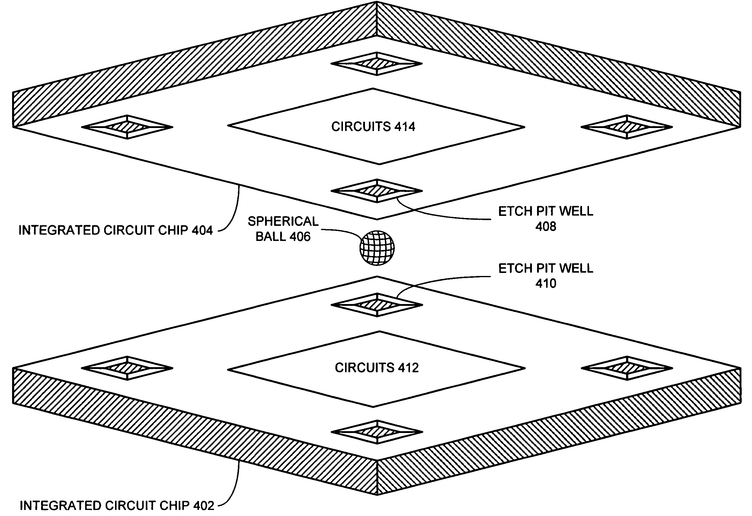
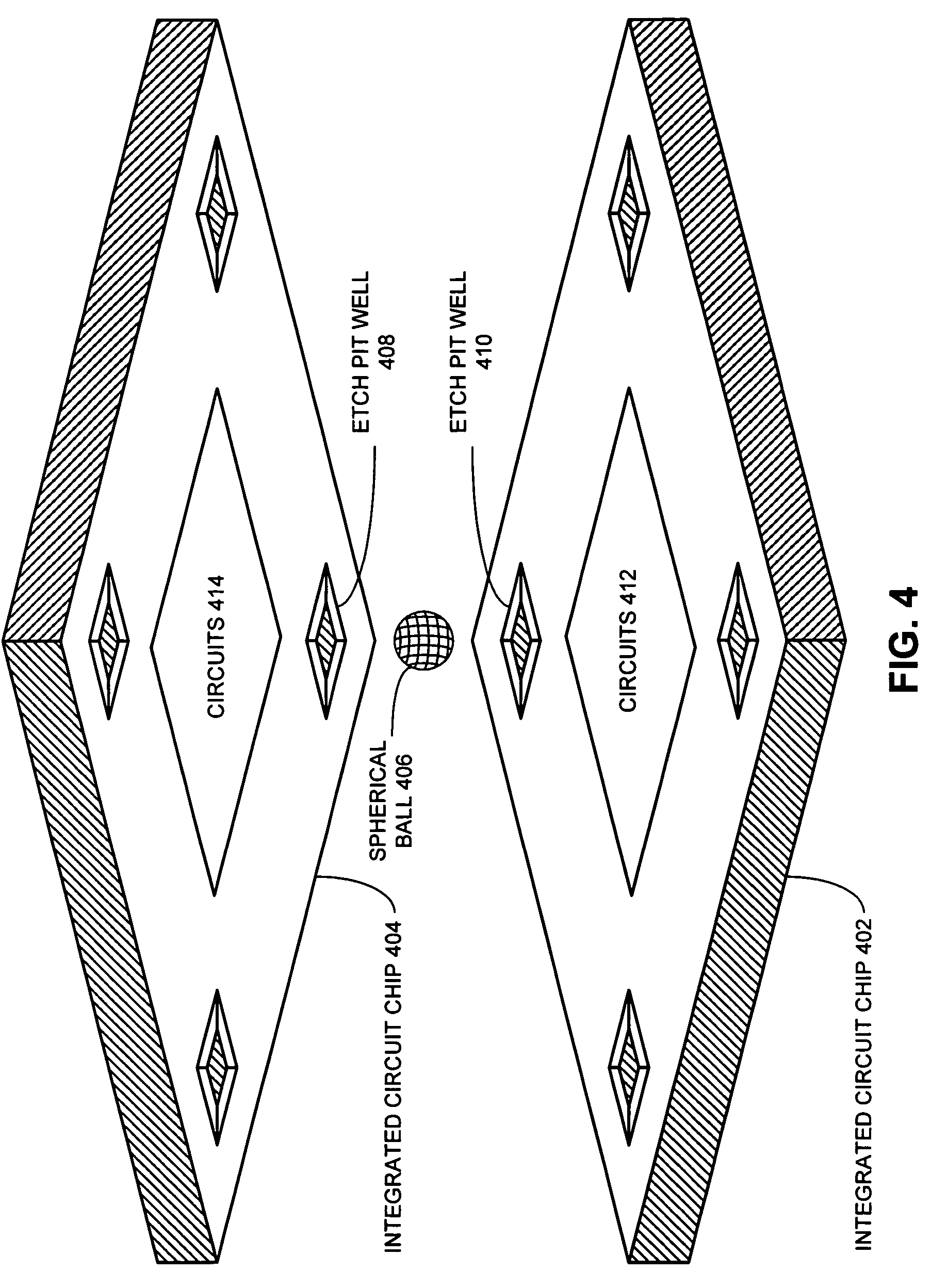
[0010]One embodiment of the present invention provides a system that facilitates precise inter-chip alignment for proximity communication and power delivery. The system includes a first integrated circuit chip, whose surface has etch pit wells. The system also includes a second integrated circuit chip, whose surface has corresponding etch pit wells configured to align with the etch pit wells of the first integrated circuit chip. A shaped structure is placed in an etch pit well of the first integrated circuit chip such that when the corresponding etch pit well of the second integrated circuit chip is substantially aligned with the etch pit well of the first integrated circuit chip, the shaped structure mates with both the etch pit well of the first integrated circuit chip and with the corresponding etch pit well of the second integrated circuit chip, thereby precisely aligning the first integrated circuit chip with the second integrated circuit chip. Besides aiding in alignment, the shaped structure also creates a conductive connection between the first integrated circuit chip and the second integrated circuit chip.
[0015]In a variation on this embodiment, the system uses compressive forces to align the first integrated circuit chip, the shaped structure, and the second integrated circuit chip. Compliance in the shaped structure and / or the etch pit wells facilitates surface contact between the shaped structure and the sidewalls or bottom of the etch pit wells.
[0017]In a variation on this embodiment, the shaped structure provides a connection that can be disconnected and reconnected easily.
[0018]In a further variation, a conductive material that reduces contact resistance is placed inside the etch pit well to increase surface contact area and reduce electrical resistance. This conductive material can include a conductive low-viscosity paste or liquid.

Problems solved by technology

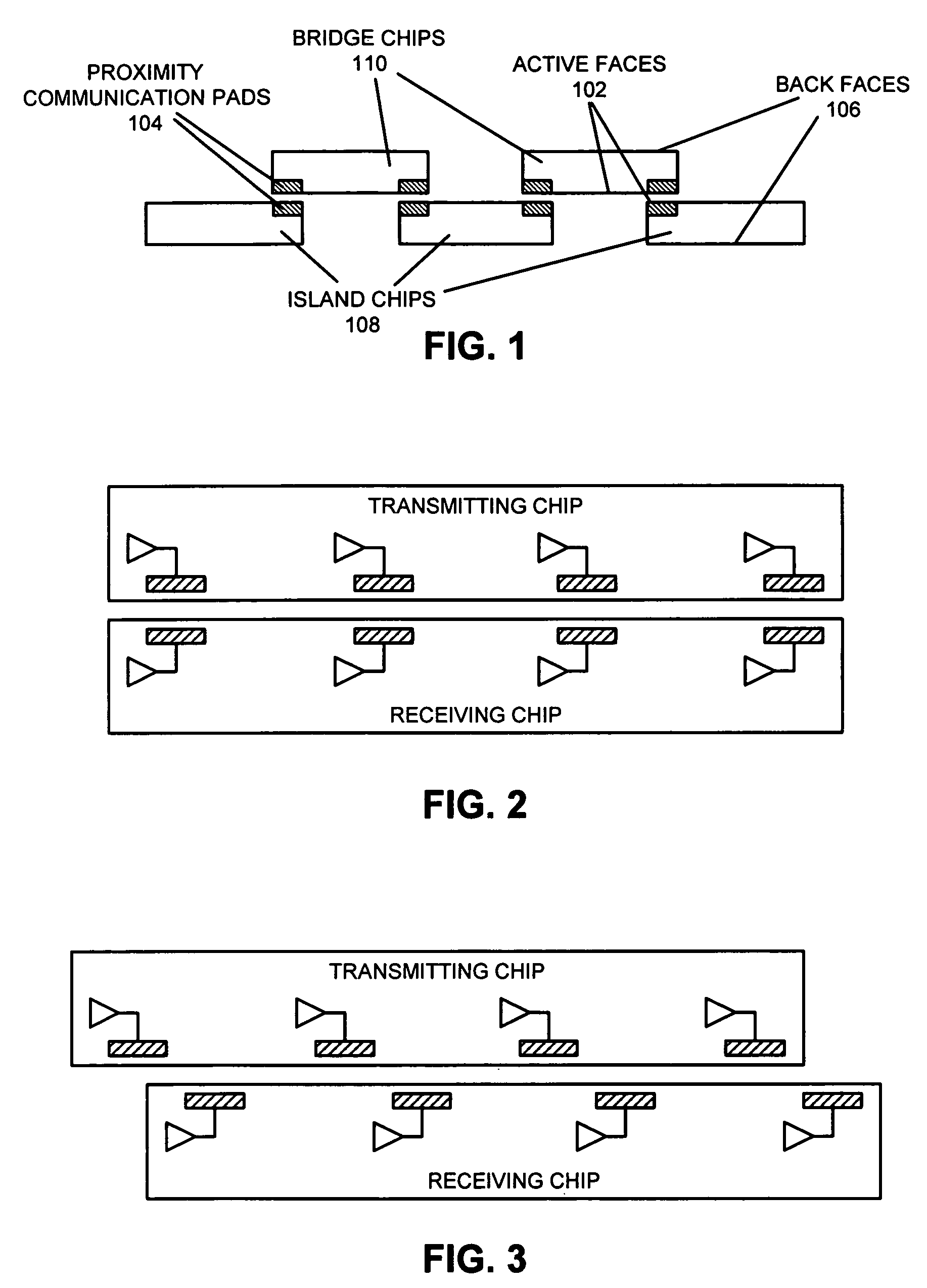
However, decreasing semiconductor line-widths and increasing on-chip clock speeds are putting pressure on the ability of traditional resistive wires to achieve the off-chip bandwidths necessary to fully utilize on-chip computational resources.
While proximity communication provides off-chip signaling bandwidth that scales with chip feature size, it also introduces topological constraints.
Achieving and maintaining chip alignment for proximity communication is challenging, especially when combined with other constraints such as conductive connections for other signals such as power and ground.

Method used


Image

  • Method and apparatus for facilitating proximity communication and power delivery
  • Method and apparatus for facilitating proximity communication and power delivery
  • Method and apparatus for facilitating proximity communication and power delivery

Examples


Embodiment Construction

[0027]The following description is presented to enable any person skilled in the art to make and use the invention, and is provided in the context of a particular application and its requirements. Various modifications to the disclosed embodiments will be readily apparent to those skilled in the art, and the general principles defined herein may be applied to other embodiments and applications without departing from the spirit and scope of the present invention. Thus, the present invention is not limited to the embodiments shown, but is to be accorded the widest scope consistent with the claims.

[0028]The data structures and code described in this detailed description are typically stored on a computer-readable storage medium, which may be any device or medium that can store code and / or data for use by a computer system. This includes, but is not limited to, magnetic and optical storage devices such as disk drives, magnetic tape, CDs (compact discs), DVDs (digital versatile discs or ...


PUM


Abstract

One embodiment of the present invention provides a system that facilitates precise inter-chip alignment for proximity communication and power delivery. The system includes a first integrated circuit chip, whose surface has etch pit wells. The system also includes a second integrated circuit chip, whose surface has corresponding etch pit wells configured to align with the etch pit wells of the first integrated circuit chip. A shaped structure is placed in an etch pit well of the first integrated circuit chip such that when the corresponding etch pit well of the second integrated circuit chip is substantially aligned with the etch pit well of the first integrated circuit chip, the shaped structure mates with both the etch pit well of the first integrated circuit chip and with the corresponding etch pit well of the second integrated circuit chip, thereby precisely aligning the first integrated circuit chip with the second integrated circuit chip. Besides aiding in alignment, the shaped structure also creates a conductive connection between the first integrated circuit chip and the second integrated circuit chip.

Description

RELATED APPLICATION[0001]This application is a continuation-in-part of pending U.S. patent application Ser. No. 11 / 243,300 filed on 3 Oct. 2005 by inventors Ashok V. Krishnamoorthy, John E. Cunningham, and Edward L. Follmer, entitled “Method and Apparatus for Precisely Aligning Integrated Circuit Chips”. This application hereby claims priority under 35 U.S.C. §120 to the above-listed parent patent application.GOVERNMENT LICENSE RIGHTS[0002]This invention was made with United States Government support under Contract No. NBCH3039002 awarded by the Defense Advanced Research Projects Administration. The United States Government has certain rights in the invention.BACKGROUND[0003]1. Field of the Invention[0004]The present invention relates generally to techniques for assembling systems containing integrated circuit chips or wafers. More specifically, the present invention relates to a method and an apparatus for precisely assembling systems containing semiconductor chips to facilitate pr...

Claims


Application Information

Patent Timeline
Patent Type & Authority Patents(United States)
IPC IPC(8): H01L23/48H01L23/52
CPCG02B6/12007H01L24/13G02B6/43H01L23/48H01L24/10H01L24/72H01L24/73H01L24/81H01L24/83H01L24/90H01L25/0657G02B6/29341H01L2224/10165H01L2224/10135H01L2224/81141H01L2224/81138H01L2224/1319H01L2224/83141H01L2924/0665H01L2924/014H01L2224/13099H01L2224/81801H01L2224/83194H01L2224/838H01L2224/83851H01L2225/06527H01L2924/01027H01L2924/01075H01L2924/01079H01L2924/10157H01L2924/14H01L2924/3011H01L2924/3025H01L2224/2919H01L2924/01006H01L2924/01023H01L2924/01033H01L2924/00H01L2924/00014H01L24/05H01L2224/05556H01L2224/05572H01L2224/05573H01L2224/056H01L2224/0615H01L2224/13
Inventor KRISHNAMOORTHY, ASHOK V.CUNNINGHAM, JOHN E.
Owner ORACLE INT CORP
Why Eureka
Eureka Blog
Learn More