Display device having optical waveguides and light-emitting units

a display device and light-emitting unit technology, applied in the field of display devices, can solve the problems of inability to use the optical waveguide display device in practical use, and inability to achieve color display

Inactive Publication Date: 2009-09-22
SEIKO EPSON CORP
View PDF9 Cites 84 Cited by
  • Summary
  • Abstract
  • Description
  • Claims
  • Application Information

AI Technical Summary

Benefits of technology

[0008]According to a first aspect of the present invention for solving the above-mentioned problems, there is provided a display device comprising a display panel having a light-emitting unit for emitting light according to predetermined display data, an elongated optical waveguide unit for guiding the light emitted from the light-emitting unit and having a core layer and an addressing unit for selecting the light from the light waveguide unit according to the predetermined display data, wherein the core layer is composed of a light scattering liquid crystal, and the addressing unit allows the light to be emitted from a predetermined part of the optical waveguide unit by using a light scattering operation of the light scattering liquid crystal.
[0009]Thereby, it is possible to improve the viewing angle characteristic or brightness characteristic of the display panel.

Problems solved by technology

However, according to the structure of the conventional display device, since the guided light has directivity in a specific direction due to the refractive index of the optical waveguide, there is a problem in that the viewing angle of the display panel becomes small.
For this reason, even though the above technology is known in the optical waveguiding display device, such an optical waveguiding display device has not been put to practical use and has not been commercialized.

Method used


Image

  • Display device having optical waveguides and light-emitting units
  • Display device having optical waveguides and light-emitting units
  • Display device having optical waveguides and light-emitting units

Examples


first embodiment

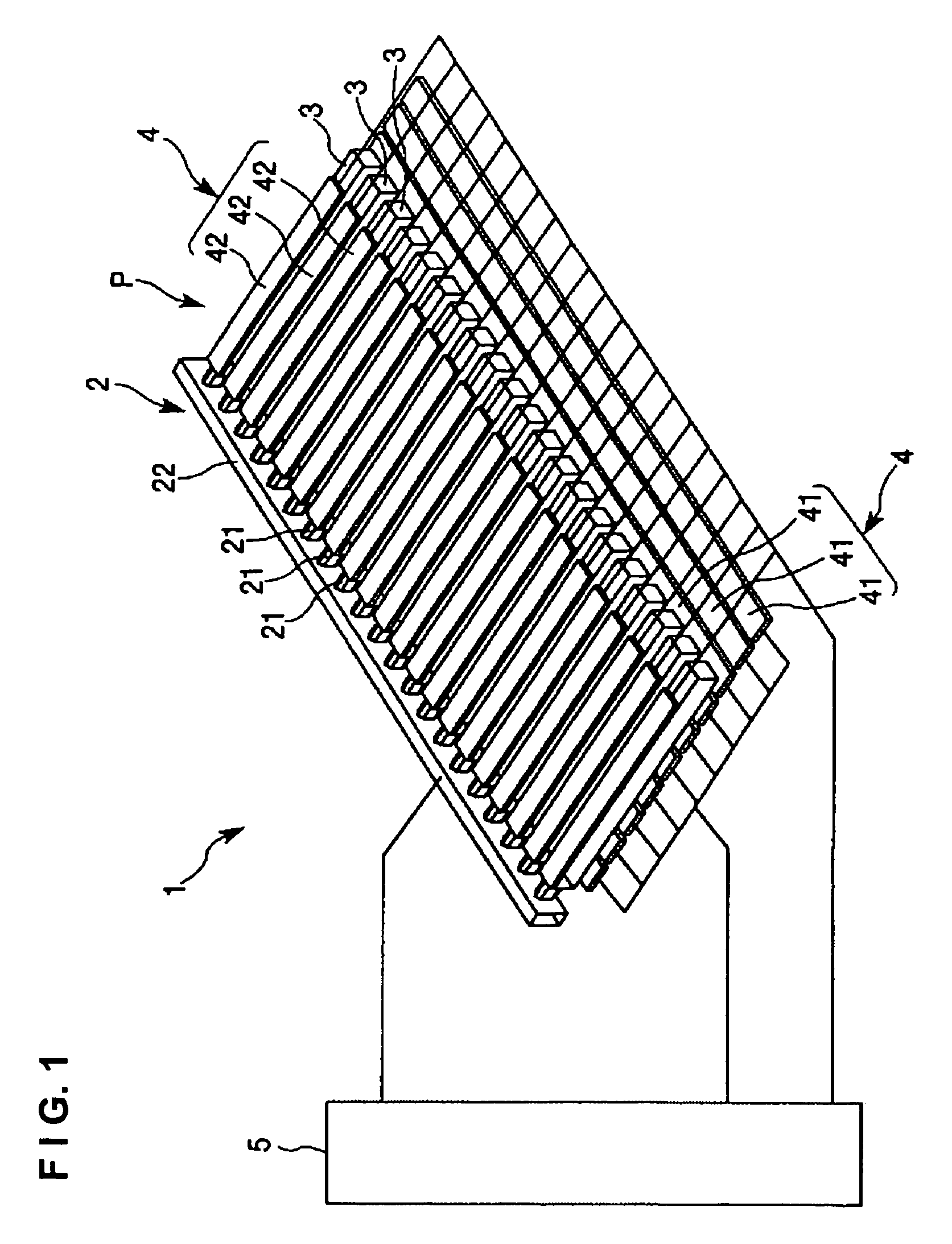
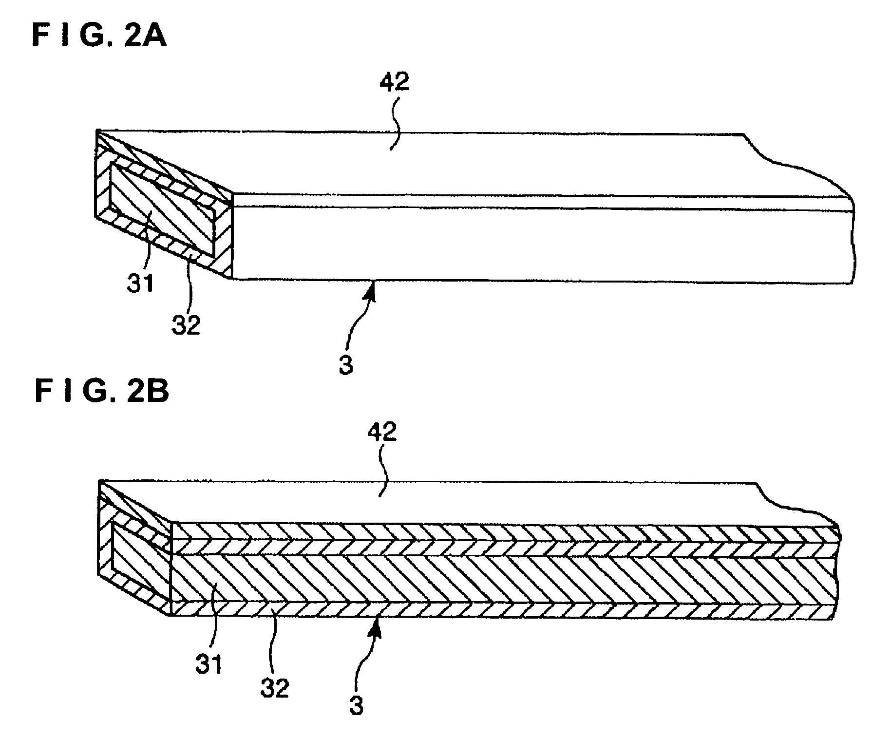
[0056]FIG. 1 is a perspective diagram illustrating a display device according to a first embodiment of the present invention. FIG. 2 is a diagram illustrating a column element of the display panel shown in FIG. 1. FIG. 2A is a perspective diagram of the column element of the display device and FIG. 2B is a cross-sectional view of the column element of the display device. The display device 1 is a flat-panel display device which is, for example, applied to electronic apparatuses such as a personal digital assistant, a game machine, a cellular phone, a personal computer, a television and the like.

[0057]Structure of Display Device

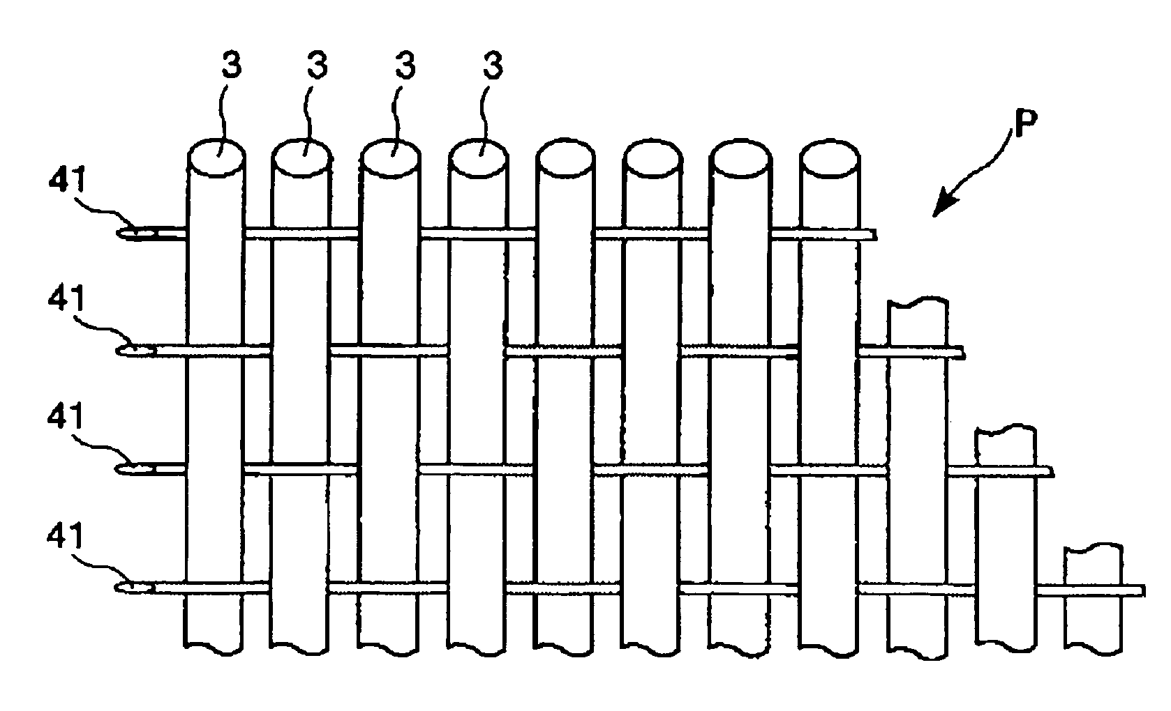
[0058]The display device comprises a light-emitting unit 2, optical waveguide units 3, addressing units 4, and a control unit 5. In the display device 1, each optical waveguide unit 3 comprises a light scattering liquid crystal 7 which will be described below, so that it is possible to improve the viewing angle of the display panel.

[0059]The light-emitting uni...

second embodiment

[0094]Structure of Display Device

[0095]FIG. 17 is a perspective diagram illustrating a display device according to a second embodiment of the present invention. FIG. 18 is a diagram illustrating the column element of the display panel shown in FIG. 17. FIG. 18A is a perspective diagram of the column element (optical waveguide unit 3) and FIG. 18B is a cross-sectional view of the column element. In addition, FIG. 19 is a diagram illustrating the row element of the display panel shown in FIG. 17. FIG. 19A is a perspective diagram of the row element (addressing unit 4) and FIG. 19B is a cross-sectional view of the row element. In the drawings described above, constituent elements of the display device 1 of the first embodiment, which are the same as those of the first embodiment, are denoted by the same reference numerals, and a description thereof is omitted. In the display device 1, each addressing unit (the column element of the display panel P) 4 is composed of the piezoelectric fi...

third embodiment

[0103]FIG. 23 is a perspective diagram illustrating a display device according to a third embodiment of the present invention. FIG. 24 is an explanatory diagram illustrating the operation of the display device shown in FIG. 23. In FIGS. 23 and 24, constituent elements of the display device 1 of the third embodiment, which are the same as those of the first embodiment, are denoted by the same reference numerals, and a description thereof is omitted. In the display device 1 according to the third embodiment, a single column electrode 47, which is obtained by combining a plurality of column electrodes, is arranged, in place of the plurality of column electrodes 42 shown in FIG. 1.

[0104]The column electrode 47 is composed of a transparent conductive material and is arranged over substantially the entire surface of the display panel P (see FIGS. 23 and 24). In addition, the column electrode 42 has flexibility and can be bent and rolled up. In addition, since the operation and relationshi...


PUM

PropertyMeasurementUnit
electric potentialaaaaaaaaaa
refractive indexaaaaaaaaaa
diameteraaaaaaaaaa

Abstract

A display device is provided that includes a display panel having a light-emitting unit for emitting light according to predetermined display data, an elongated optical waveguide unit which guides the light incident from the light-emitting unit and has a core layer and an addressing unit for selecting the light from the light waveguide unit according to the predetermined display data. The core layer is composed of light scattering liquid crystal, and the addressing unit allows the light to be emitted from a predetermined part of the optical waveguide unit by using the light scattering operation of the light scattering liquid crystal.

Description

RELATED APPLICATIONS[0001]This application claims priority to Japanese Patent Application No. 2004-027344 filed Feb. 3, 2004 which is hereby expressly incorporated by reference herein in its entirety.BACKGROUND[0002]1. Technical Field[0003]The present invention relates to a display device.[0004]2. Related Art[0005]Conventionally, a display device has a refractive index changing unit provided on an external surface of an optical waveguide (optical fiber). The refractive index changing unit has the optical waveguide arranged therebetween and applies a voltage to the optical waveguide when the display device is driven. In this case, at a part of the optical waveguide to which the voltage is applied, the reflective index is changed by a Kerr effect, and the light transmitted to the optical waveguide is guided to the outside of the optical waveguide. As a result, the display panel emits the light (for example, see Japanese Patent Laid-Open No. 59-148030)).[0006]In the above conventional ...

Claims


Application Information

Patent Timeline
Patent Type & Authority Patents(United States)
IPC IPC(8): G09G3/34G09G3/36G02F1/13G02B6/04G02F1/1333G02F1/1334G02F1/139G02F1/19G09F9/30
CPCG02F1/1326G02B6/04
Inventor KATASE, MAKOTO
Owner SEIKO EPSON CORP
Why Eureka
Try Eureka