Thin film resistor and method of forming the resistor on spaced-apart conductive pads

a technology of conductive pads and thin films, which is applied in the direction of resistors, resistors, adjustable resistors, etc., can solve the problem of difficult control of the resistance provided by resistors

Active Publication Date: 2009-12-15
NAT SEMICON CORP
View PDF3 Cites 18 Cited by
  • Summary
  • Abstract
  • Description
  • Claims
  • Application Information

AI Technical Summary

Problems solved by technology

As a result, it becomes difficult to contr

Method used


Image

  • Thin film resistor and method of forming the resistor on spaced-apart conductive pads
  • Thin film resistor and method of forming the resistor on spaced-apart conductive pads
  • Thin film resistor and method of forming the resistor on spaced-apart conductive pads

Examples


Embodiment Construction

[0019]FIGS. 6A-6B to 17A-17B show a series of views that illustrate an example of a method 200 of forming a thin film resistor in accordance with the present invention. FIGS. 6A-17A show a series of plan views, while FIGS. 6B-17B show a series of cross-sectional views. As described in greater detail below, the present invention forms a thin film resistor on a pair of spaced-apart conductive pads which, in turn, allows electrical contacts to be made to the conductive pads rather than directly to the resistor.

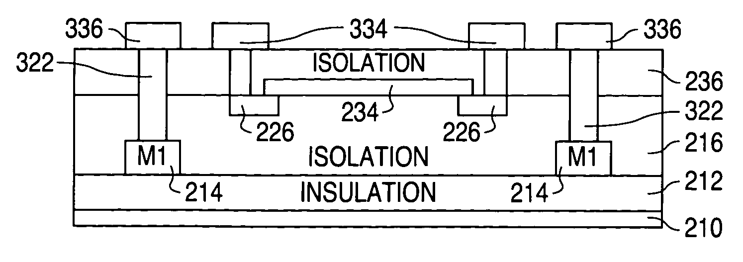
[0020]As shown in the FIGS. 6A-6B example, method 200 utilizes a semiconductor wafer 210 which has been conventionally processed to form layer of insulation material 212 on semiconductor wafer 210, a number of metal-1 traces 214 that have been formed on insulation layer 212, and a layer of isolation material 216 that has been formed on insulation layer 212 and the metal-1 traces 214. Isolation layer 216, which has been planarized, can be formed to have a thickness of, for example...


PUM


Abstract

A thin film resistor is formed to have very accurately defined dimensions which, in turn, allow the resistive value of the resistor to be very accurately defined. The resistor is formed on spaced-apart conductive pads which, in turn, are electrically connected to conductive plugs that are spaced apart from the resistor.

Description

BACKGROUND OF THE INVENTION[0001]1. Field of the Invention[0002]The present invention relates to thin film resistors and, more particularly, to a thin film resistor and method of forming the resistor on spaced-apart conductive pads.[0003]2. Description of the Related Art[0004]A thin film resistor is a structure that is formed from a conducting resistive material. As with conventionally-formed discrete resistors, thin film resistors are formed to provide a predefined resistance to the flow of current through the semiconductor structure.[0005]FIGS. 1A-1B to 5A-5B show a series of views that illustrate a prior-art method 100 of forming a thin film resistor. FIGS. 1A-5A show a series of plan views, while FIGS. 1B-5B show a series of corresponding cross-sectional views. As shown in FIGS. 1A-1B, method 100 begins with a conventionally-formed layer of insulation material 110, and continues with the deposition of a thin layer of resistor material 112, such as a layer of silicon carbide chro...

Claims


Application Information

Patent Timeline
IPC IPC(8): H01C10/00
CPCH01C7/006H01C17/28H01C17/075
Inventor JOHNSON, PETERDE SANTIS, JOSEPH A.FOOTE, JR., RICHARD WENDELL
Owner NAT SEMICON CORP
Why Eureka
Try Eureka