Semiconductor electromechanical contact

a technology of electromechanical contact and semiconductor, which is applied in the direction of electrical equipment, printed circuits, coupling device connections, etc., can solve the problems of small space available, extremely small travel, and rapid wear of load boards

Inactive Publication Date: 2010-04-13
XCERRA
View PDF46 Cites 26 Cited by
  • Summary
  • Abstract
  • Description
  • Claims
  • Application Information

AI Technical Summary

Benefits of technology

[0011]The two cantilevered beams are compressed as they slide against one another and increase travel distances up to 0.035 inches of travel. The two plungers can be offset or aligned in the slots in the housing. Another advantage of the present invention is that it eliminates the multiple wiping that occurs on the load board. When the cantilever beams are compressed, the test pad on the load board is wiped once and held in contact as multiple integrated circuits are tested.
is that it eliminates the multiple wiping that occurs on the load board. When the cantilever beams are compressed, the test pad on the load board is wiped once and held in contact as multiple integrated circuits are tested.

Problems solved by technology

Disadvantages with the design embodied in the '629 patent is that the contact provides an extremely small amount of travel, 0.008 inches, which leaves little room for error.
This is particularly problematic when you consider there is a very small amount of room available for interconnection between the leads on an integrated circuit and the contact pads on the load board.
A second disadvantage is that the load board is quickly worn out because of wiping action of the device at both the integrated circuit lead and the load board pads.
Considering the integrated circuits are continually cycling through the test and being changed a single wipe is advantageous, however, the load board is continually used throughout the repeated testing of integrated circuits and therefore the constant wiping wears out the load board.

Method used


Image

  • Semiconductor electromechanical contact
  • Semiconductor electromechanical contact
  • Semiconductor electromechanical contact

Examples


Embodiment Construction

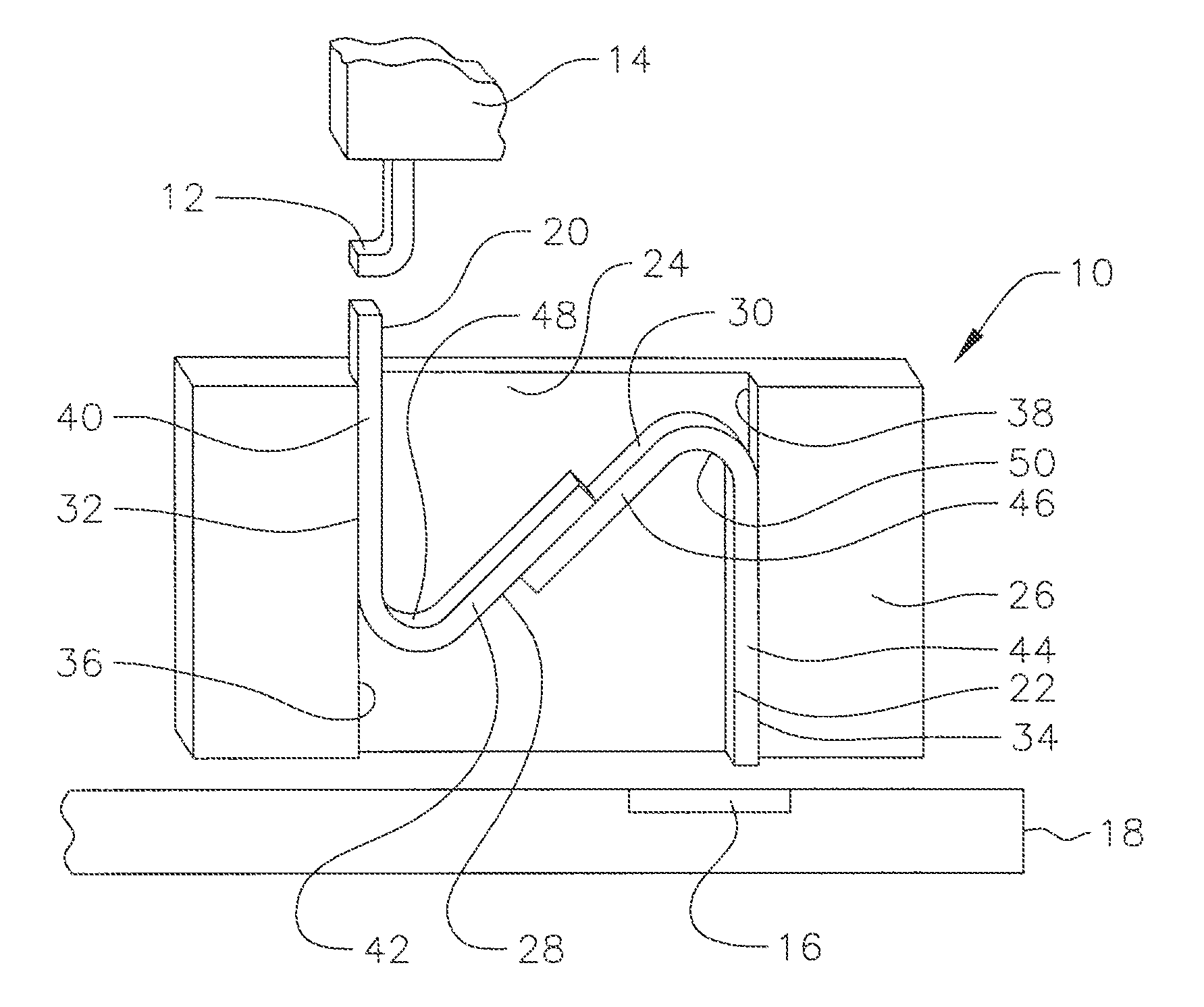
[0017]Referring to FIG. 1, a compliant semiconductor electromechanical contact assembly 10 of the present invention is illustrated. The assembly 10 is for interconnecting a lead or terminal 12 of an integrated circuit 14 or other device to a corresponding terminal spaced a distance apart from the integrated circuit. For example, in FIG. 1, the terminal is a test pad 16 on a printed circuit board, commonly known as a load board 18. The assembly 10 comprises pairs of cantilever beams 20 and 22 positioned within a slot 24 in a housing 26. It is to be understood that although housing 26 illustrates a single slot 24 and one pair of cantilever beams 20, 22, there can be multiple pairs of cantilever beams in spaced apart slots within housing 26 depending upon the number of leads 12 for a particular integrated circuit 14 being tested. Beams 20 and 22 are arranged within the slot 24 such that a portion of sliding surfaces 28 and 30 slide along one another during compression of the beams. The...


PUM


Abstract

A compliant electrical contact assembly for interconnecting a lead or terminal of an integrated circuit having two cantilever beams positioned within a slot in a housing arranged such that a portion of the beams slide along a portion of one another and within the housing as the beams are deformed elastically in order to allow more travel and compliance without yielding or totally deforming the beam. The sliding action during deformation effectively multiplies the total compliance in the assembly above and beyond the compliance otherwise available to elastic compression of the cantilever beams.

Description

CROSS-REFERENCE TO RELATED APPLICATION(S)[0001]This application claims priority to U.S. provisional application Ser. No. 60 / 973,358 filed Sep. 18, 2007.FIELD OF THE INVENTION[0002]The present invention relates to the field of electrical interconnect systems and more specifically to a device for interconnecting the leads of an integrated circuit with corresponding terminals on a printed circuit board interfacing with a tester intended to effect test analysis of the integrated circuit device.BACKGROUND OF THE INVENTION[0003]Many applications exist for effecting electrical contact between two conductors. An application includes interconnection between the leads of an integrated circuit device and conductive pads or terminals on a printed circuit board which serves as an interface between the integrated circuit device under test and the tester apparatus.[0004]Both electrical and mechanical considerations are necessary to design an interconnect between an integrated circuit and the print...

Claims


Application Information

Patent Timeline
Patent Type & Authority Patents(United States)
IPC IPC(8): H01R12/00
CPCH01R12/714H01R13/2407H01R2107/00H01R13/2435H01R13/2428
Inventor SWART, MARKELLIS, JOHN
Owner XCERRA
Why Eureka
Try Eureka