

Pixel circuit
a pixel circuit and circuit technology, applied in the field of pixel circuits, can solve the problems of increasing power consumption, reducing gate voltage, and reducing brightness, and achieve the effects of reducing drive current, excellent brightness uniformity, and large parasitic capacitan
- Summary
- Abstract
- Description
- Claims
- Application Information
AI Technical Summary
Benefits of technology
Problems solved by technology
Method used
Image

Examples
Embodiment Construction
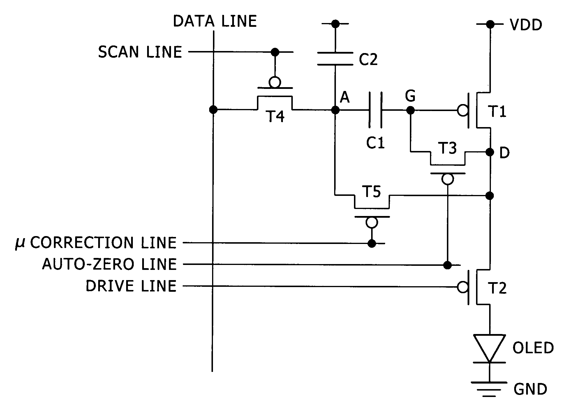
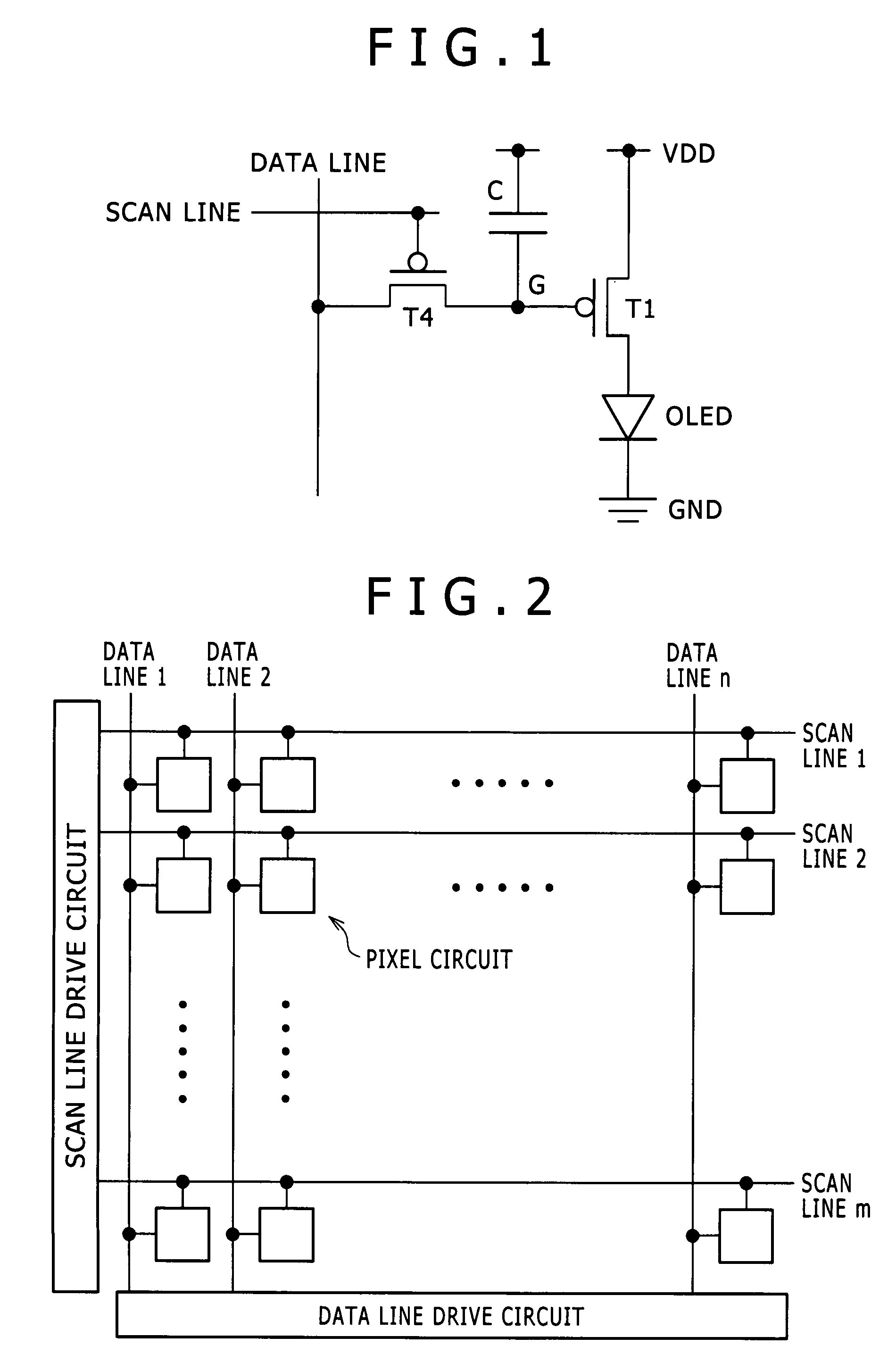
[0035]Preferred embodiments of the present invention will be described in detail below with reference to the accompanying drawings. FIG. 2 is a block diagram illustrating the overall configuration of an image display apparatus having a pixel circuit associated with an embodiment of the present invention which is integrated into an IC. As shown in the figure, the image display apparatus includes a pixel array unit in the center and a data line drive circuit and a scan line drive circuit which are provided around the pixel array unit. The pixel array unit includes scan lines 1 to m arranged in row directions, data lines 1 to n arranged in column directions, and pixel circuits each disposed where a scan line and a data line intersect each other. The scan line drive circuit is connected to the scan lines 1 to m and sequentially supplies a control signal for linear sequential scanning of the same circuits. The data line drive circuit is connected to the data lines 1 to n. and supplies a ...
PUM
 Abstract
Description
Claims
Application Information