Amplifier circuit with reduced phase noise

一种放大器电路、电流镜的技术,应用在放大器、差分放大器、直流耦合的直流放大器等方向,能够解决输出信号不能轨对轨延伸、没有提供相位噪音降级的避免等问题,达到减少时间、电流迅速减小的效果

Active Publication Date: 2010-10-13
THE SWATCH GRP RES & DEVELONMENT LTD
View PDF6 Cites 6 Cited by
  • Summary
  • Abstract
  • Description
  • Claims
  • Application Information

AI Technical Summary

Problems solved by technology

However, with this type of structure, the output signal cannot extend rail-to-rail as in the present invention
In addition, no protection against phase noise degradation is provided, which constitutes another disadvantage

Method used


Image

  • Amplifier circuit with reduced phase noise
  • Amplifier circuit with reduced phase noise
  • Amplifier circuit with reduced phase noise

Examples


Embodiment Construction

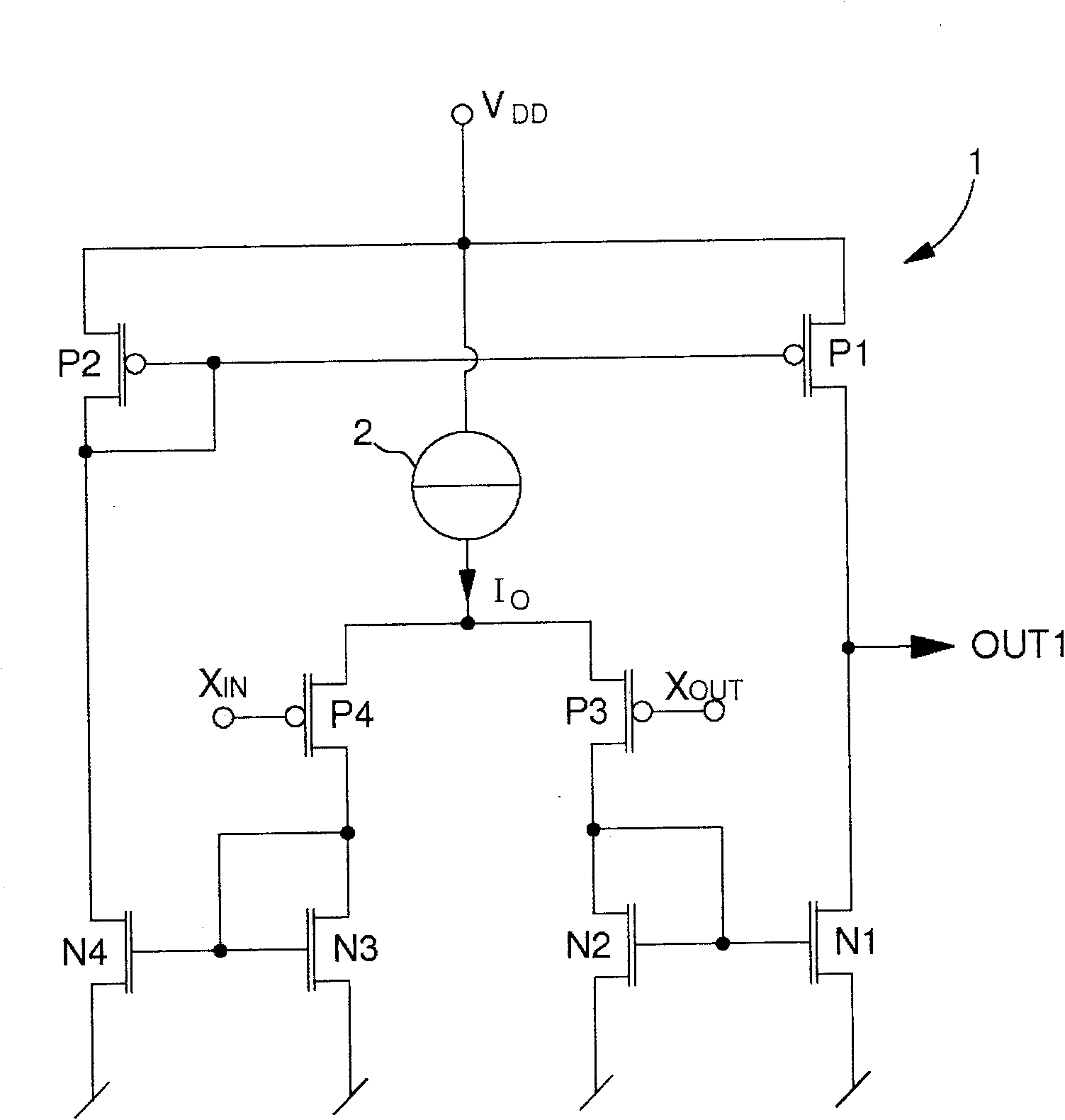
[0024]In the following description, elements of the amplifier circuit which are known to a person skilled in the art will only be referred to in a simplified manner, in particular with regard to how the individual transistors of the amplifier circuit are produced. The amplifier circuit of the present invention is mainly used to supply at least one clock or time base signal based on an inverted oscillation signal from a crystal oscillator in electronic equipment. The transistors described below are preferably MOS transistors, however, it is also conceivable to manufacture the amplifier circuit with bipolar transistors or a combination of MOS and bipolar transistors. At this point, note that each PMOS transistor presented below defines a MOS transistor having a first type of conductivity, while each NMOS transistor defines a MOS transistor having a second type of conductivity, although the reverse is also conceivable .

[0025] figure 2 A first embodiment of the low noise amp...


PUM


Abstract

The amplifier circuit (1) includes a differential pair of PMOS transistors at input (P3, P4), whose source receives a current from a current source (3). The gate of the first transistor (P3) of the pair defines a non-inverting input (XOUT) and the gate of the second transistor (P4) of the pair defines an inverting input (XIN). A drain of the first transistor (P3) of the differential pair is connected to a diode connected NMOS transistor (N2) of a first current mirror (N1, N2), and a drain of the second transistor (P4) of the differential pair is connected to a diode connected NMOS transistor (N3) of a second current mirror (N3, N4). A diode connected PMOS transistor (P2) of a third current mirror is connected to the drain of a second NMOS transistor (N4) of the second current mirror, while a drain of a second PMOS transistor (P1) of the third current mirror is connected to the drain of a second NMOS transistor (N1) of the first current mirror to define a first output (OUT1), which is inverted by a reverser (N5, P7) to supply an inverted output signal (OUT) capable of varying rail to rail. A first complementary NMOS transistor (N6) is connected in the form of a reverser with the first PMOS transistor (P3) of the differential pair. A second complementary NMOS transistor (N7) is connected in the form of a reverser with the second MOS transistor (P4) of the differential pair.

Description

technical field [0001] The present invention relates to low phase noise amplifier circuits, in particular for supplying at least one clock or time base signal. Such an amplifier circuit - which may be an operational transconductance amplifier circuit - comprises a differential pair of MOS or bipolar transistors on the input, a first and a second current mirror connected to the transistors of the differential pair and a third current mirror connected to the first and second current mirrors between the two terminals of the supply voltage source. The connection node between the first and third current mirror supplies an output signal whose level extends over the entire supply voltage range. Background technique [0002] The amplifier circuit of the present invention can be regarded as a buffer circuit. This type of buffer circuit is an intermediate amplifier circuit which is arranged between, for example, a quartz oscillator transmitting two or one oscillation signals in oppo...

Claims


Application Information

Patent Timeline
Patent Type & Authority Applications(China)
IPC IPC(8): H03F3/45H03F1/26
CPCH03F2203/45674H03F3/45183H03F2203/45664H03F2203/45476H03F2203/45366
Inventor C·贝拉斯克斯
Owner THE SWATCH GRP RES & DEVELONMENT LTD
Why Eureka
Try Eureka