Display Device Driving Circuit, Data Signal Line Driving Circuit, and Display Device

a technology of driving circuit and display device, applied in the direction of electric digital data processing, instruments, computing, etc., can solve the problem of large electric power consumption of the driving circuit of the liquid crystal display device, and achieve the effect of suppressing the current occurring

Inactive Publication Date: 2009-07-02
SHARP KK
View PDF14 Cites 6 Cited by
  • Summary
  • Abstract
  • Description
  • Claims
  • Application Information

AI Technical Summary

Benefits of technology

[0018]As is clear from the above, the rise time becomes longer as the amplitude of an input voltage is smaller. This can be understood as follows. More specifically, when an input voltage has a small amplitude, for example when a High voltage is supplied via an input terminal IN and a Low voltage is supplied via an inverted input terminal INB, a gate voltage (=a voltage across gate and source) of an n-channel MOS transistor 205 is 2 V. This 2 V is not different than a large amplitude but a gate voltage (=a voltage across gate and source) of a p-channel MOS transistor 204 decreases. Therefore, a drain current of the p-channel MOS transistor 204 is suppressed small. This causes an increase in time required for the drain current to charge a capacitor load connected to the output terminal OUT, thereby resulting in that the voltage outputted via the output terminal OUT slowly rises.
[0025]According to the invention, a driving circuit of a display device includes connection and disconnection means. Therefore, when a voltage, having a DC level which varies in accordance with an input signal, is outputted as an output voltage from the analog amplifier circuit, it is possible for the connection and disconnection means to (i) break an electrical connection between an output of the analog amplifier circuit and an input of a digital circuit until the output voltage rises or falls to a target DC level, and (ii) make the electrical connection between the output of the analog amplifier circuit and the input of the digital circuit after the output voltage has risen or fallen to the target DC level. This allows the DC level which has risen or fallen to be supplied, as the output voltage of the analog amplifier circuit, to a CMOS circuitry included in the digital circuit. It follows that no output voltage during a rise period or a fall period of the analog amplifier circuit is supplied to the CMOS circuitry. Therefore, it is possible to suppress a through current occurring in the CMOS circuitry.

Problems solved by technology

However, the following problems occur in the conventional liquid crystal display device.
A problem occurs that the driving circuit of the liquid crystal display device has great electric power consumption, thus caused by the through current flowing in the digital circuit.

Method used


Image

  • Display Device Driving Circuit, Data Signal Line Driving Circuit, and Display Device
  • Display Device Driving Circuit, Data Signal Line Driving Circuit, and Display Device
  • Display Device Driving Circuit, Data Signal Line Driving Circuit, and Display Device

Examples


Embodiment Construction

[0051]One embodiment of the present invention is described below with reference to FIGS. 1 through 10.

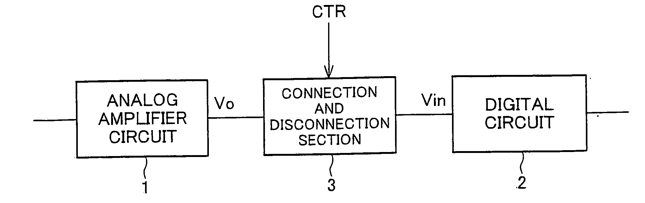
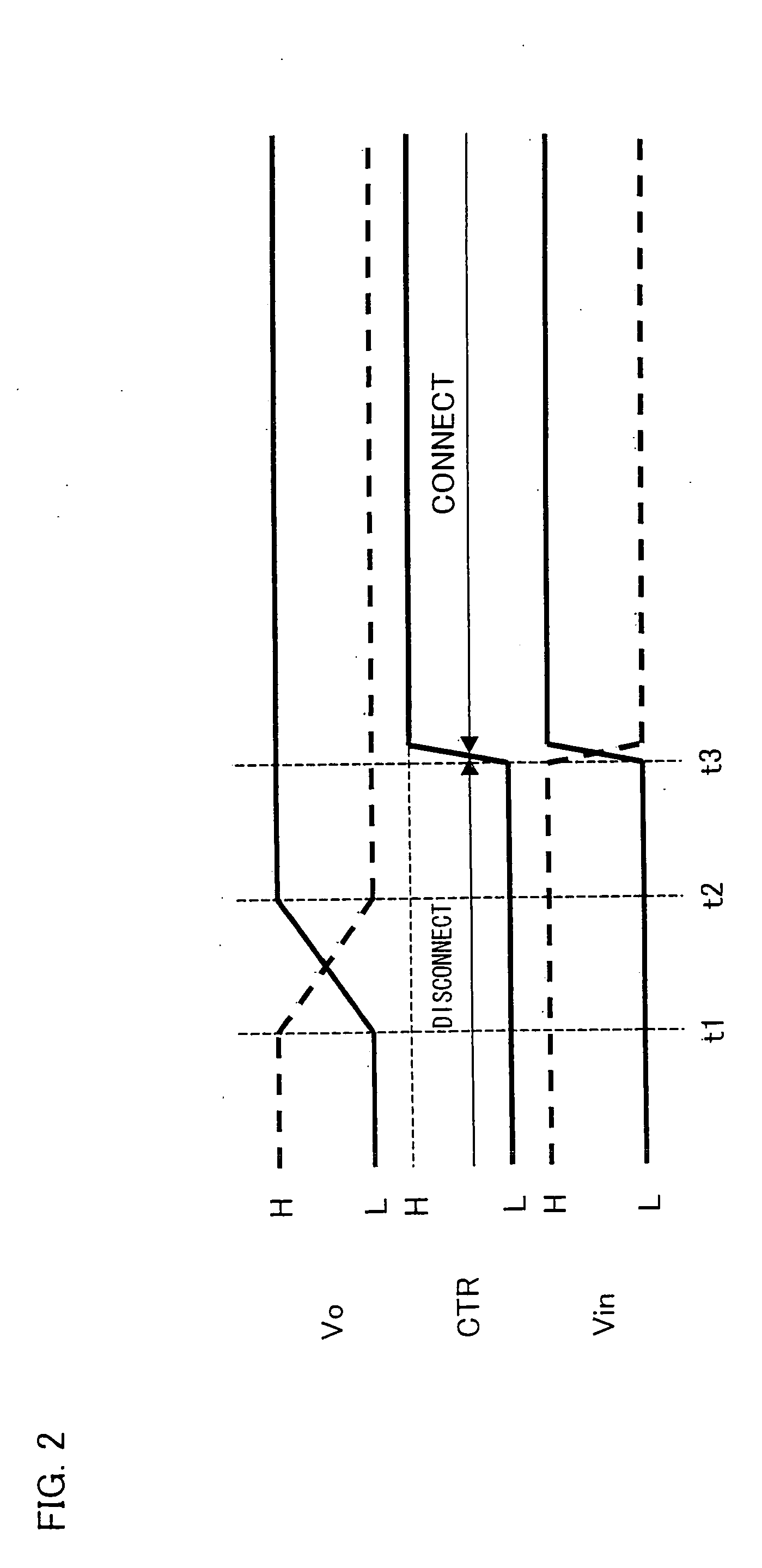
[0052]In the BACKGROUND ART, it is explained that data signal line driving circuits and scanning signal driving circuits of liquid crystal display devices include various circuit configurations in which a digital circuit, including a CMOS circuitry, by which an analog amplifier circuit is followed. In this circuit configuration, the analog amplifier circuit outputs a DC level in accordance with an input signal, and the CMOS circuitry included in the digital circuit receives an output voltage of the analog amplifier circuit. Instead, the present embodiment provides a circuit configuration as shown in FIG. 1.

[0053]FIG. 1 illustrates a circuit configuration in which a connection and disconnection section (connection and disconnection means) 3 is provided between (a) an output terminal of an analog amplifier circuit 1 in which a DC level which varies in accordance with an input signal i...


PUM


Abstract

In one embodiment of the present invention, a driving circuit is disclosed of a display device, a connection and disconnection section is provided between an output of an analog amplifier circuit and an input of a digital circuit. The connection and disconnection section breaks an electrical connection between the output of the analog amplifier circuit and the input of the digital circuit until an output voltage of the analog amplifier circuit rises to a target DC level, and makes an electrical connection between the output of the analog amplifier circuit and the input of the digital circuit after the output voltage of the analog amplifier circuit has risen to the target DC level.

Description

TECHNICAL FIELD[0001]The present invention relates to a circuit configuration for use in a driving circuit for a display device, in which driving circuit an analog circuit is followed by a digital circuit.BACKGROUND ART[0002]Liquid crystal display devices have been manufactured in which a driving circuit for a liquid crystal panel and the liquid crystal panel are monolithically formed by use of a polysilicon. A polysilicon thin film transistor has a higher threshold voltage than a transistor which uses a single-crystal silicon. Therefore, liquid crystal panels which use the polysilicon, generally, drives the polysilicon thin film transistor after carrying out a level shift with respect to a signal voltage to be supplied to the driving circuit.[0003]Patent Document 1 discloses a liquid crystal display device which carries out such a level shift. A liquid crystal display device illustrated in FIG. 11 is introduced in Patent Document 1 as a well-known technique.[0004]In the liquid crys...

Claims


Application Information

Patent Timeline
Patent Type & Authority Applications(United States)
IPC IPC(8): G09G5/00G09G3/36
CPCG09G3/3406G09G3/3688G09G2360/144G09G2320/0626G09G2330/021G09G2310/0289
Inventor NAKAGAWA, YOUSUKESHIMIZU, SHINSAKUSAKAI, TAMOTSU
Owner SHARP KK
Why Eureka
Try Eureka