Eureka AIR delivers breakthrough ideas for toughest innovation challenges, trusted by R&D personnel around the world.

Processing method for wafer and processing apparatus therefor

a processing method and wafer technology, applied in the field of processing methods and processing apparatuses, can solve the problems of difficult handling of semiconductor wafers, insufficient heat resistance of protective tapes, and easy cracking of semiconductor wafers, and achieve the effect of reliably transfer and convenient handling

Active Publication Date: 2010-12-28
DISCO CORP
View PDF8 Cites 6 Cited by
  • Summary
  • Abstract
  • Description
  • Claims
  • Application Information

AI Technical Summary

Benefits of technology

[0011]Therefore, an object of the present invention is to provide a processing method and a processing apparatus which can reliably transfer a wafer from a process for removing a peripheral reinforcing portion of the wafer to a process for dividing of the wafer into devices (for example, semiconductor chips) without damage occurring in the wafer.
[0013]In the processing method of the present invention, after a necessary portion (at least the projection) of the peripheral reinforcing portion is removed, in order to transfer the wafer to a next process, while the wafer is not separated from the holding table and the wafer is held on the holding table, the holding tape supported by the frame is applied onto the rear surface of the wafer. Since the holding tape is applied on the wafer, the wafer can be transferred to the next process via the frame without contacting the wafer directly by handing device. Therefore, the wafer, which is thinned by the removal of the peripheral reinforcing portion and may not be thereby easily handled, can be reliably transferred without damage thereto.
[0015]In the wafer of which the projection of the peripheral reinforcing portion will be removed in the above processing method of the present invention, the rigidity can be secured by the peripheral reinforcing portion, so that the handleability and the durability can be improved. Therefore, since heat due to deposition, sputtering, or the like cause no problem, a metal film may be provided to a region of the rear surface which corresponds to the device region.
[0016]When at least the projection of the peripheral reinforcing portion is removed, ground waste or the like may be generated, and may be adhered to the rear surface of the wafer. Thus, if the holding tape is applied on the rear surface in the above condition of the wafer, the following problem may be caused when the wafer is divided into devices in a process after the transferring. That is, since the holding tape closely contacts the holding table, the surface of the wafer is cut, and the wafer is divided into devices, the wafer cannot closely contact the holding table and cannot be held thereby due to the ground waste which is adhered to the rear surface of the wafer and exists in the holding tape. As a result, the wafer may be rickety, so that the wafer cannot be reliably cut. In order to solve this problem, after the peripheral reinforcing portion is removed, the wafer may be subjected to the cleaning while the wafer is held on the holding table. After the cleaning, the holding tape may be applied to the rears surface of the wafer, so that the above problem can be prevented.
[0019]In the present invention, after a necessary portion (at least the projection) of the peripheral reinforcing portion is removed, in order to transfer the wafer to a next process, while the wafer is not separated from the holding table and the wafer is held on the holding table, the holding tape supported by the frame is applied onto the rear surface of the wafer, and the wafer is transferred to the next process via the frame. Therefore, the wafer, which is thinned by the removal of the peripheral reinforcing portion and may not be thereby easily handled, can be reliably transferred without damage thereto.

Problems solved by technology

Due to this, it is difficult to handle the semiconductor wafer after the thinning, and cracking easily occurs in the semiconductor wafer.
However, when a metal film composed of gold is provided by a method (for example, deposition or sputtering) on a rear surface of the semiconductor wafer after thinning, the protective tape has insufficient heat-resistance, so that the processing temperature needed to be lower.
Due to this, processing is more time-consuming in this case than in normal cases.
However, when the semiconductor wafer has the above peripheral reinforcing portion, it is difficult to stably hold the semiconductor wafer.
However, since this modification of the chuck table is not practical, the above peripheral reinforcing portion of the semiconductor wafer is removed, so that the entire semiconductor wafer is processed to have a plate shape.
However, in this case, since the peripheral reinforcing portion of the wafer is removed, the rigidity of the wafer is low and damage (for example, cracking) easily occurs in the wafer.

Method used


Image

  • Processing method for wafer and processing apparatus therefor
  • Processing method for wafer and processing apparatus therefor
  • Processing method for wafer and processing apparatus therefor

Examples


Embodiment Construction

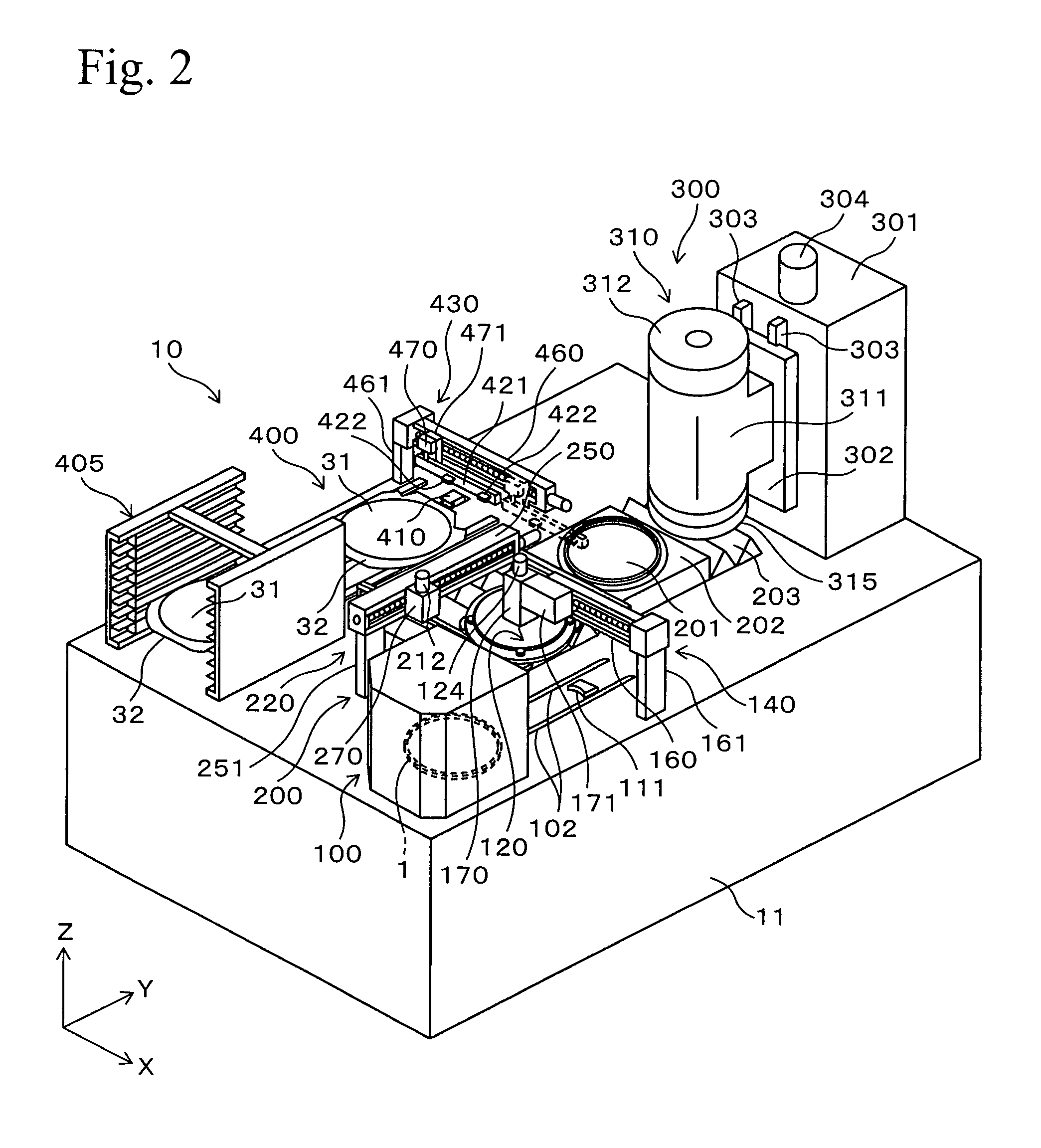
[0033]An embodiment of the present invention will be explained hereinafter with reference to the drawings.

1. Semiconductor Wafer

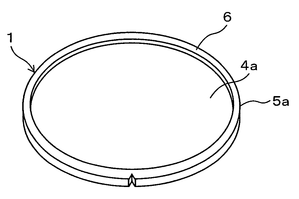
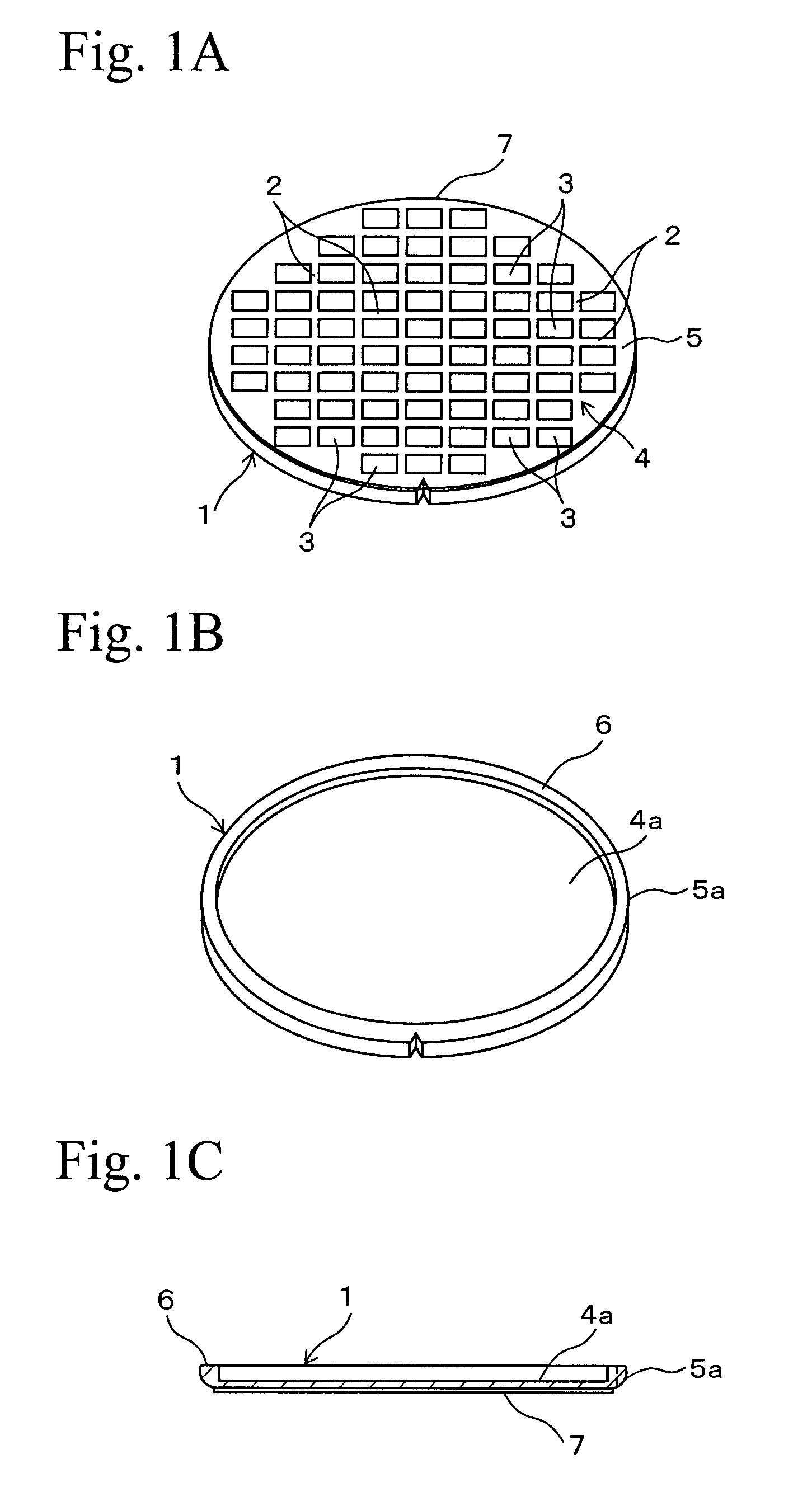
[0034]In FIGS. 1A to 1C, reference numeral 1 denotes a disc-shaped semiconductor wafer (hereinafter referred to simply as “wafer”) which is processed in the embodiment. The wafer 1 is a silicon wafer or the like. As shown in FIG. 1A, grid-like predetermined division lines 2 are formed on a surface of the wafer 1, and plural rectangular semiconductor chips 3 are defined by the predetermined division lines 2 on the surface of the wafer 1. Electronic circuits (for example, Integrated Circuits (ICs) and Large Scale Integrations (LSIs)), which are not shown in FIGS. 1A to 1C, are formed on surfaces of the semiconductor chips 3. The plural semiconductor chips 3 are formed on a device region 4 which is almost circular so as to be concentric with the wafer 1. A ring-shaped peripheral extra region 5, which has no semiconductor chip 3 formed thereon, is formed around...


PUM

PropertyMeasurementUnit
thicknessaaaaaaaaaa
thicknessaaaaaaaaaa
abrasive grain diameteraaaaaaaaaa

Abstract

A processing method for a wafer includes: preparing a wafer which has a device region having plural devices formed on a surface of the wafer; and a peripheral reinforcing portion which is integrally formed around the device region and has a projection projecting outwardly on a rear surface of the wafer. The processing method further includes: removing at least the projection of the peripheral reinforcing portion of the wafer; and transferring the wafer after the removing. In the removing, while the wafer is held on a holding table such that the rear surface of the wafer is exposed and the surface of the wafer closely contacts the holding table, at least the projection of the peripheral reinforcing portion is removed. After the removing of at least the projection, while the wafer is held on the holding table, a holding tape is applied to the rear surface of the wafer and the holding tape is supported by a frame. In the transferring, the wafer having the holding tape applied thereon is separated together with the frame from the holding table and is transferred together with the frame.

Description

[0001]This application claims priority under 35 U.S.C. §119 to Japanese Patent Application No. JP2006-090235 filed Mar. 29, 2006, the entire content of which is hereby incorporated by reference.BACKGROUND OF THE INVENTION[0002]1. Field of the Invention[0003]The present invention relates to a processing method and to a processing apparatus in which a thick peripheral reinforcing portion of a wafer (for example, a semiconductor wafer), which is formed around a region of the wafer having devices (for example, semiconductor chips) formed thereon, is removed from the wafer and the wafer is transferred to a next process.[0004]2. Description of Related Art[0005]In general, semiconductor chips, which are used in various electronic apparatuses, are produced by the following method. That is, grid-like rectangular regions are defined by predetermined division lines on a disc-shaped semiconductor wafer, and electronic circuits are formed on surfaces of the rectangular regions. Next, a rear surf...

Claims


Application Information

Patent Timeline
Patent Type & Authority Patents(United States)
IPC IPC(8): H01L21/302C03C25/68
CPCH01L21/3043H01L21/67132H01L21/6836H01L21/78H01L2221/68327
Inventor KAJIYAMA, KEIICHIMASUDA, TAKATOSHI
Owner DISCO CORP
Why Eureka
Eureka Blog
Learn More