
Eureka
For R&D, Eureka makes reading and utilizing patents & technical documents easy.
Eureka AIR
Designed for self-driven R&D workflows. Generate viable solutions, solve complex R&D challenges, empower your innovation with AI.

Eureka Materials
Designed for material experts only. Revolutionize your material R&D, from search, analyze, to developing new materials.

TechResearch
Generate reliable direction feasibility study reports for your R&D in just a few steps.

TechSeek
Discover and master advanced knowledge NOW. Basics, ideas, possibilities, all at once.

TechMind
As an expert in R&D Theories, TechMind can generates customized viable solutions instantly.

TechRisk
Analyze your overall solution with one click, know your potential R&D risks in advance.

TechMonitor
Get weekly tech updates, stay abreast of the latest tech innovations and key insights.
Substrate attracting device and substrate transfer apparatus
- Summary
- Abstract
- Description
- Claims
- Application Information
AI Technical Summary
Benefits of technology
Problems solved by technology
Method used
Image

Examples
Embodiment Construction
[0025]Hereinafter, embodiments of the present invention will be described with reference to FIGS. 1A to 4B which form a part hereof. However, the present invention is not limited thereto.
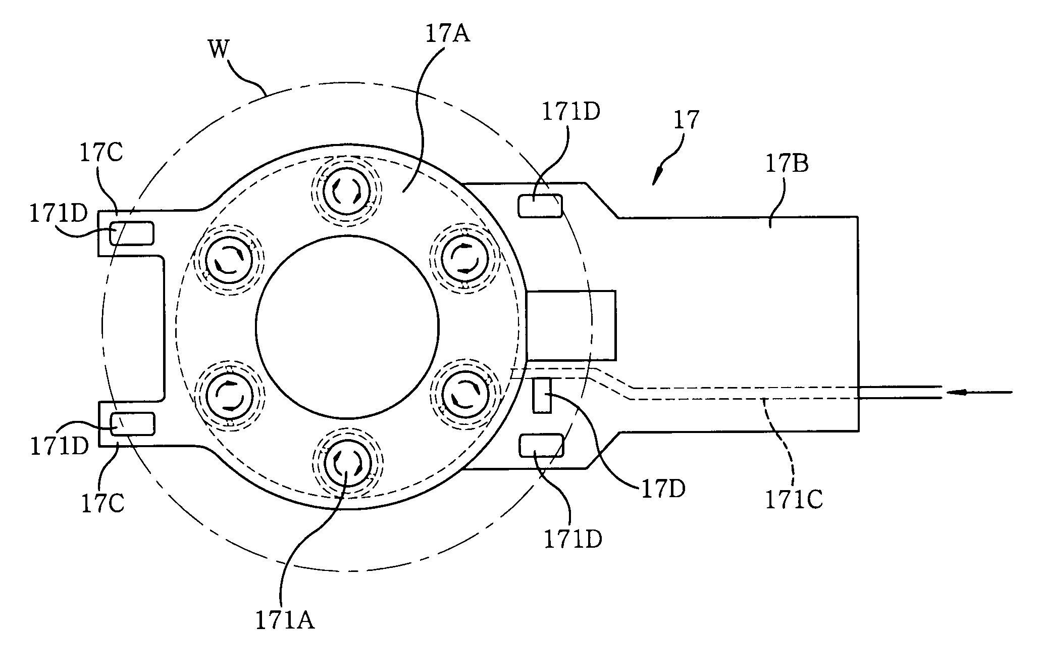
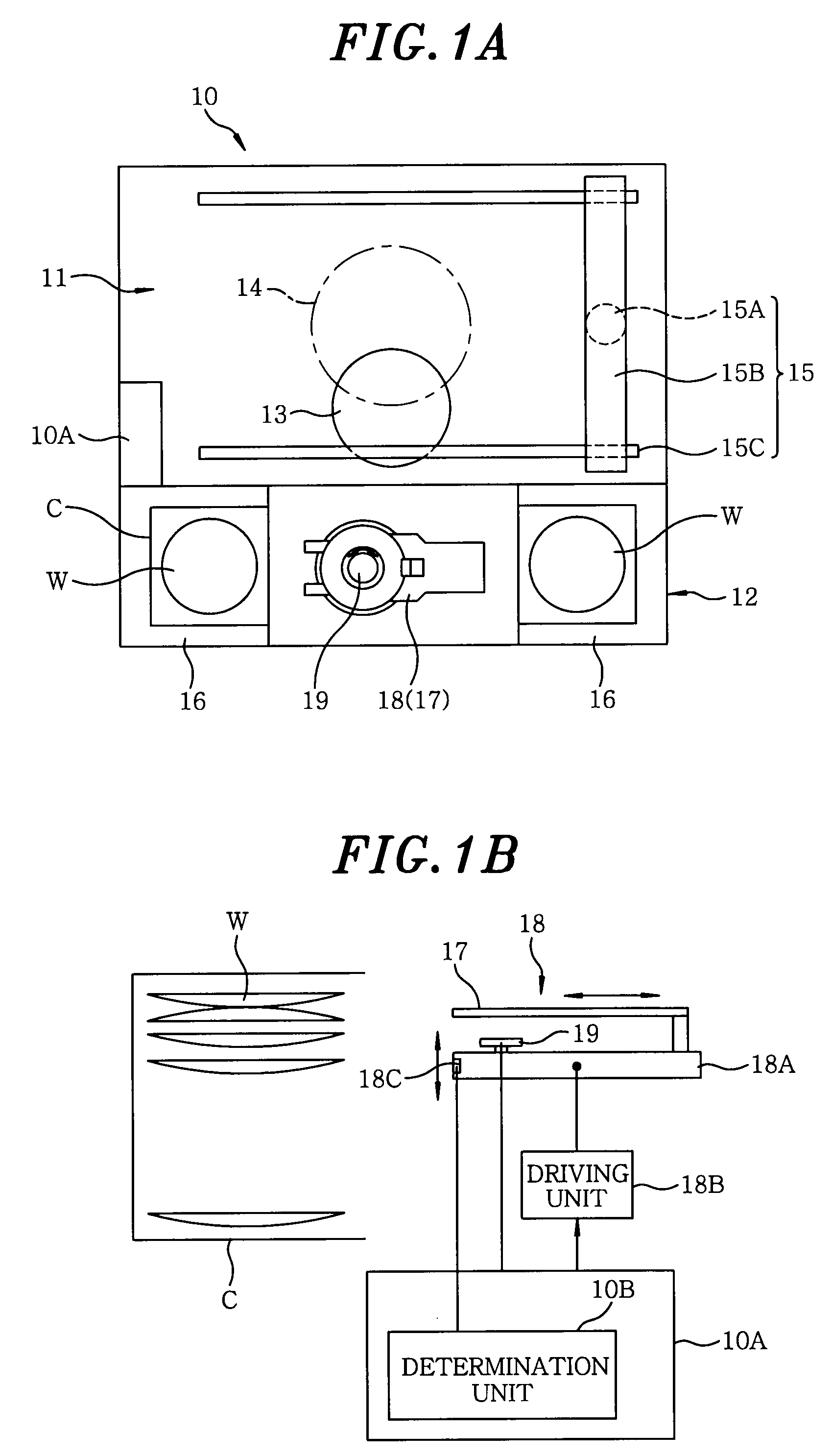
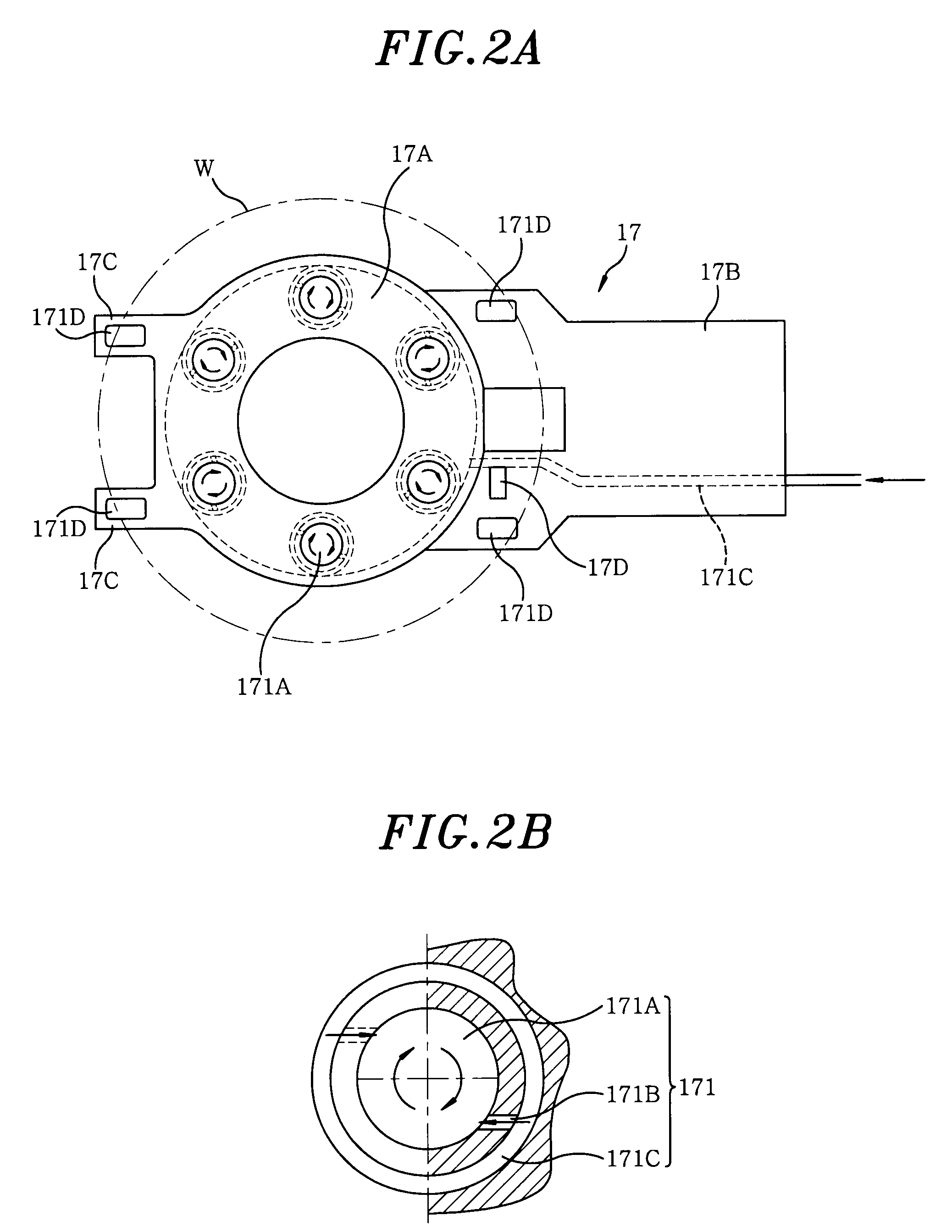
[0026]As shown in FIG. 1A by way of example, an inspection apparatus 10 in accordance with the embodiment of the present invention includes a probe chamber 11 for inspecting electrical characteristics of a substrate (e.g., a semiconductor wafer) W and a loader chamber 12 provided adjacent to the probe chamber 11 for transferring the semiconductor wafer W. Various kinds of units and mechanisms of the probe chamber 11 and the loader chamber 12 are controlled by a controller 10A.
[0027]As can be seen in FIGS. 1A and 1B, the probe chamber 11 includes a main chuck 13 for mounting a semiconductor wafer W thereon, the main chuck 13 being movable in X, Y and Z directions, a probe card 14 arranged above the main chuck 13 and an alignment mechanism 15 for bringing a plurality of probes (not shown) of the probe...
PUM
 Abstract
Description
Claims
Application Information
 - R&D Engineer
- R&D Manager
- IP Professional
- Industry Leading Data Capabilities
- Powerful AI technology
- Patent DNA Extraction
Browse by: Latest US Patents, China's latest patents, Technical Efficacy Thesaurus, Application Domain, Technology Topic, Popular Technical Reports.
© 2024 PatSnap. All rights reserved.Legal|Privacy policy|Modern Slavery Act Transparency Statement|Sitemap|About US| Contact US: help@patsnap.com