Semiconductor device

a technology of semiconductor devices and devices, applied in the field of semiconductor device design technology, can solve the problems of abnormal operation of semiconductor devices, non-target values, and failure of semiconductor devices to normally perform objective operation

Active Publication Date: 2011-01-11
SK HYNIX INC
View PDF6 Cites 4 Cited by
  • Summary
  • Abstract
  • Description
  • Claims
  • Application Information

AI Technical Summary

Benefits of technology

[0030]Also, some embodiments of the present invention are directed to providing a semiconductor device capable of preventing an internal circuit from being initialized during the wafer burn-in test by inactivating an internal reset signal generated in response to a reset signal inputted from the outside through a reset input pad even if the externally inputted reset signal is in an activated state in the wafer burn-in test.

Problems solved by technology

However, when the semiconductor device performs the objective operation by using the electric signal, a noise or a spark is generated in the used electric signal for unaccountable reason and thus an error may occur preventing the semiconductor device from normally performing the objective operation.
Besides, when a power-up operation is performed by initially supplying a power to the semiconductor device, a voltage level or a logic level of an internally used electric signal may not have a target value.
However, when the semiconductor device is operated, the semiconductor device may be abnormally operated for an unpredictable reason in unpredictable circumstances.
In this case, the reset signal defined by the MRS cannot be properly activated, and as a result, the abnormal operation of the semiconductor device may not be prevented.
Meanwhile, generally, the semiconductor device is mass-produced through very complicated and difficult processes.
As a matter of course, while the semiconductor device is mass-produced, a defective semiconductor device, which cannot be operated for the original purpose, is always manufactured because of variations of the manufacturing process.
Although the semiconductor device which cannot be operated for the original purpose like this should be distinguished from the normally operated semiconductor device, it is not easy to determine whether the semiconductor device is normally operated or not since the semiconductor device is generally small-sized and highly integrated.
No matter how precisely the electric signal are supplied to the predetermined pads location-wise, the neighboring other pads may also be supplied with a significant amount of the electric signal and thus a result of the wafer burn-in test may be inaccurate.
Particularly, in case of resetting the whole semiconductor device in response to the external reset signal OUT_RESETb inputted from the outside through the reset input pad 100 such as the semiconductor device shown in FIG. 1, because of the external reset signal OUT_RESETb inputted with a wrong logic level from the outside of the semiconductor through the reset input pad 100, a problem of incorrectly resetting the semiconductor device may occur.

Method used


Image

  • Semiconductor device
  • Semiconductor device
  • Semiconductor device

Examples


first embodiment

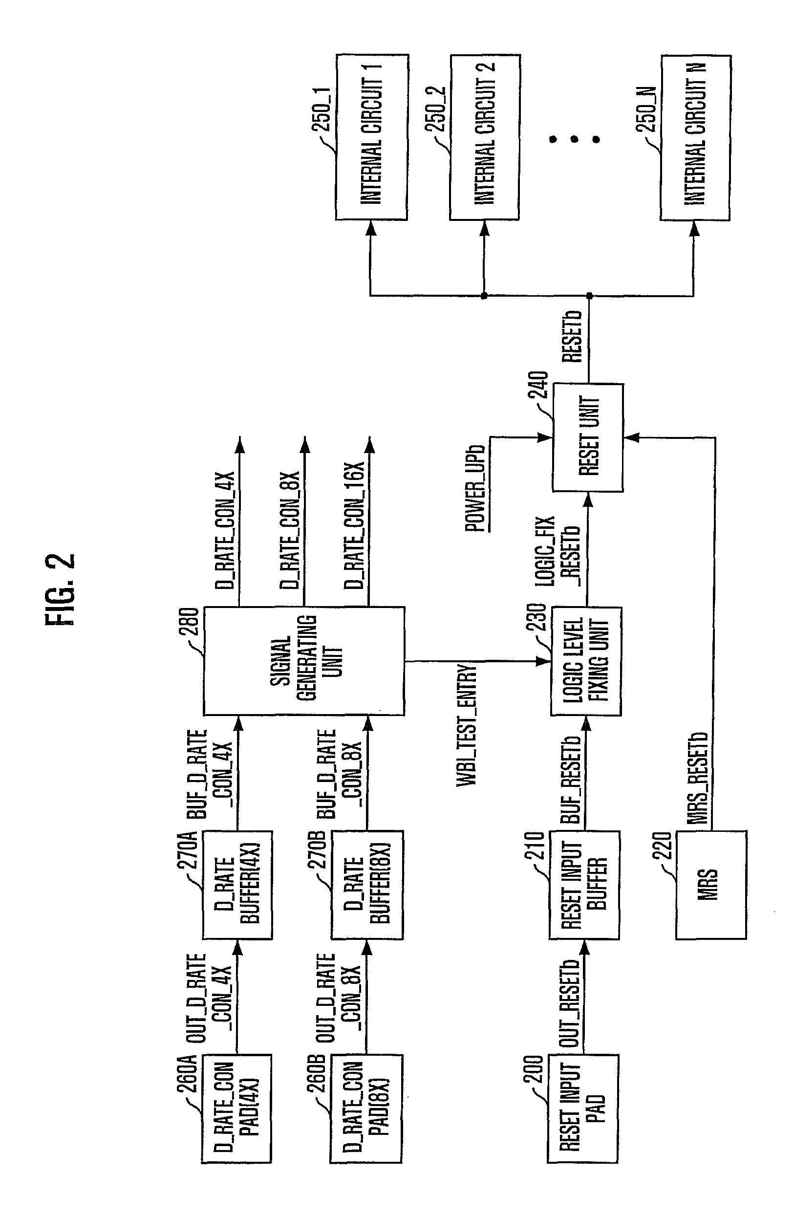
[0039]FIG. 2 is a block diagram for explaining an operation of filtering a reset signal inputted from the outside through a reset input pad when a wafer burn-in test is performed in a semiconductor device in accordance with a first embodiment of the present invention.

[0040]As shown, the semiconductor device in accordance with the first embodiment of the present invention includes a signal generating unit 280, a logic level fixing unit 230, and a reset unit 240.

[0041]The signal generating unit 280 generates signals D_RATE_CON—4X, D_RATE_CON—8X and D_RATE_CON—16X for adjusting a data input / output bandwidth or for generating a test signal WBI_TEST_ENTRY for controlling an entry into a test mode in response to signals OUT_D_RATE_CON—4X and OUT_D_RATE_CON—8X inputted from the outside through predetermined first pads 260A and 260B.

[0042]The logic level fixing unit 230 fixes an external reset signal OUT_RESETb applied through a predetermined second pad 200, i.e., a reset input pad, to a pr...

second embodiment

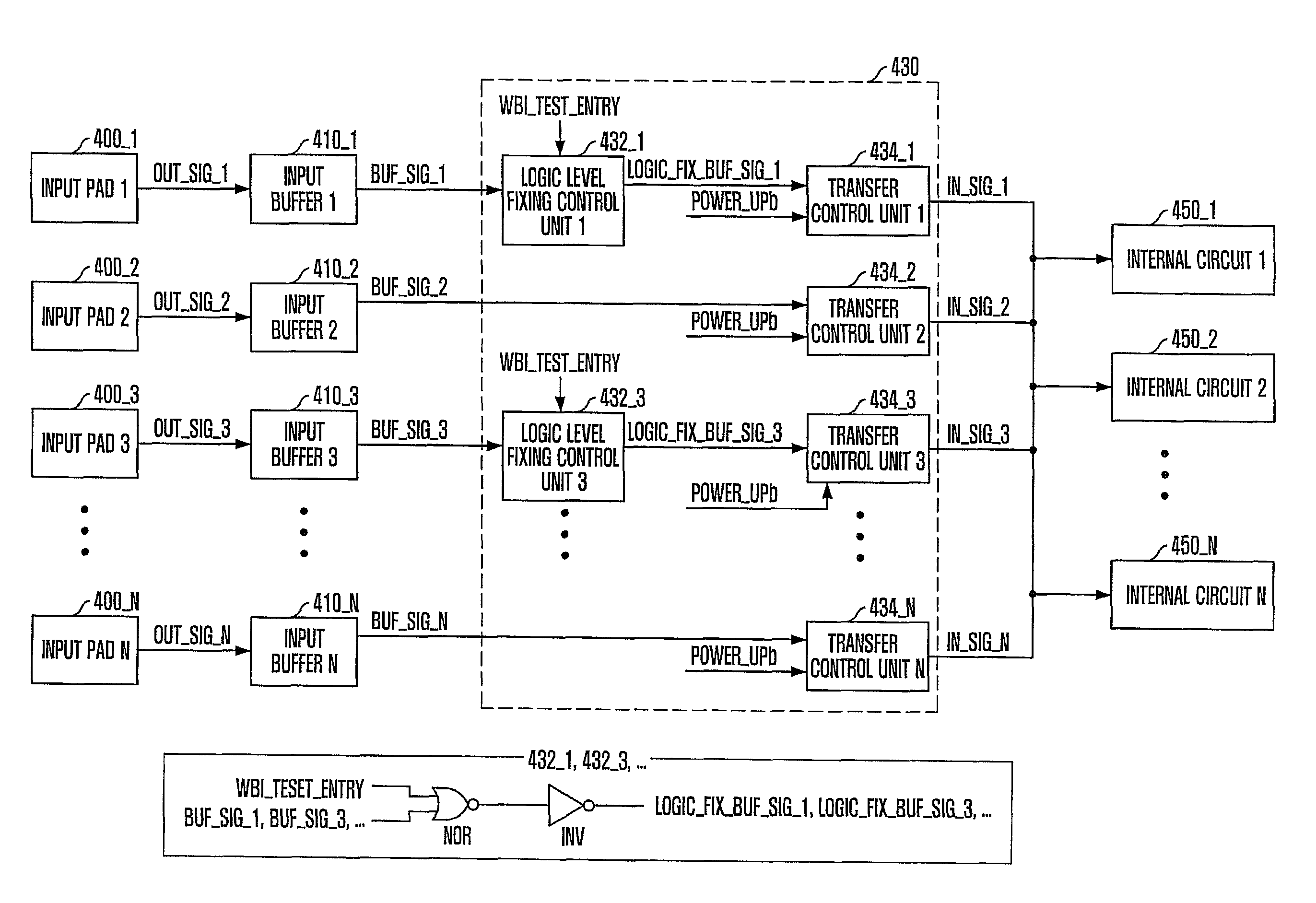
[0076]FIG. 4 is a block diagram for explaining an operation of filtering an electric signal falsely inputted to an internally provided pad when a wafer burn-in test mode operation is performed in a semiconductor device in accordance with a second embodiment of the present invention.

[0077]As shown, the semiconductor device in accordance with the second embodiment of the present invention includes a plurality of input pads 400_1 to 400_N for receiving a plurality of external signals OUT_SIG_1 to OUT_SIG_N; a plurality of internal circuits 450_1 to 450_N for performing a predetermined internal operation in response to the external signals OUT_SIG_1 to OUT_SIG_N inputted through the plurality of input pads 400_1 to 400_N; and a signal transferring unit 430 for fixing the external signals OUT_SIG_1, OUT_SIG_3 and etc. inputted through predetermined input pads 400_1, 400_3 and etc. among the plurality of input pads 400_1 to 400_N at a predetermined logic level and transferring the fixed s...


PUM


Abstract

A semiconductor device includes a plurality of pads configured to receive a plurality of external signals, an internal circuit configured to perform a predetermined internal operation in response to one of the external signals that is inputted through one of the plurality of pads, and a signal transferring unit configured to receive the external signal, output the external signal to an internal circuit an output signal during a normal mode, and output a fixed signal regardless of changes in the external signal to the internal circuit in a test mode.

Description

CROSS-REFERENCE TO RELATED APPLICATION[0001]The present invention claims priority of Korean patent application number 10-2008-0110066, filed on Nov. 6, 2008 which is incorporated by reference in its entirety.BACKGROUND OF THE INVENTION[0002]The present invention relates to a semiconductor design technology, and more particularly, to a semiconductor device capable of preventing a voltage level of a pad which is not used in a wafer burn-in test mode operation from being floated.[0003]Generally, a semiconductor device uses a method of performing an objective operation through an operation of receiving or outputting a plurality of electric signals which swing within a predetermined range of a voltage level.[0004]At this time, the plurality of electric signals which swing within the predetermined range of a voltage level may be a power supply voltage or an internal voltage fixed to a particular voltage level for operating an internal circuit of the semiconductor device in an analog aspec...

Claims


Application Information

Patent Timeline
Patent Type & Authority Patents(United States)
IPC IPC(8): H03K19/00
CPCG01R31/318511G11C29/06G11C29/1201G11C29/48G11C29/006G11C29/14G11C2207/105
Inventor YUN, TAE-SIKLEE, KANG-SEOL
Owner SK HYNIX INC
Why Eureka
Try Eureka