Flip-chip packages allowing reduced size without electrical shorts and methods of manufacturing the same

a technology of flip-chip and packaging, which is applied in the field of flip-chip packages, can solve the problems of difficulty in forming flip-chip packages with a fine pitch, limited reduction of pitch, and frequent and achieve the effect of preventing electrical shorts between conductive bumps

Inactive Publication Date: 2011-02-01
SAMSUNG ELECTRONICS CO LTD
View PDF8 Cites 104 Cited by
  • Summary
  • Abstract
  • Description
  • Claims
  • Application Information

AI Technical Summary

Benefits of technology

[0008]Example embodiments may provide flip-chip packages that are capable of preventing electrical shorts between conductive bumps without expanding the size of a substrate.

Problems solved by technology

As a result, because the pitch between the second pads of the substrate is very narrow, electrical shorts between the conductive bumps may frequently occur.
However, reducing the pitch has some limitations.
Therefore, the electrical shorts may act as limitations in reducing the size of the substrate so that forming the flip-chip package having a fine pitch may be difficult.

Method used


Image

  • Flip-chip packages allowing reduced size without electrical shorts and methods of manufacturing the same
  • Flip-chip packages allowing reduced size without electrical shorts and methods of manufacturing the same
  • Flip-chip packages allowing reduced size without electrical shorts and methods of manufacturing the same

Examples


Embodiment Construction

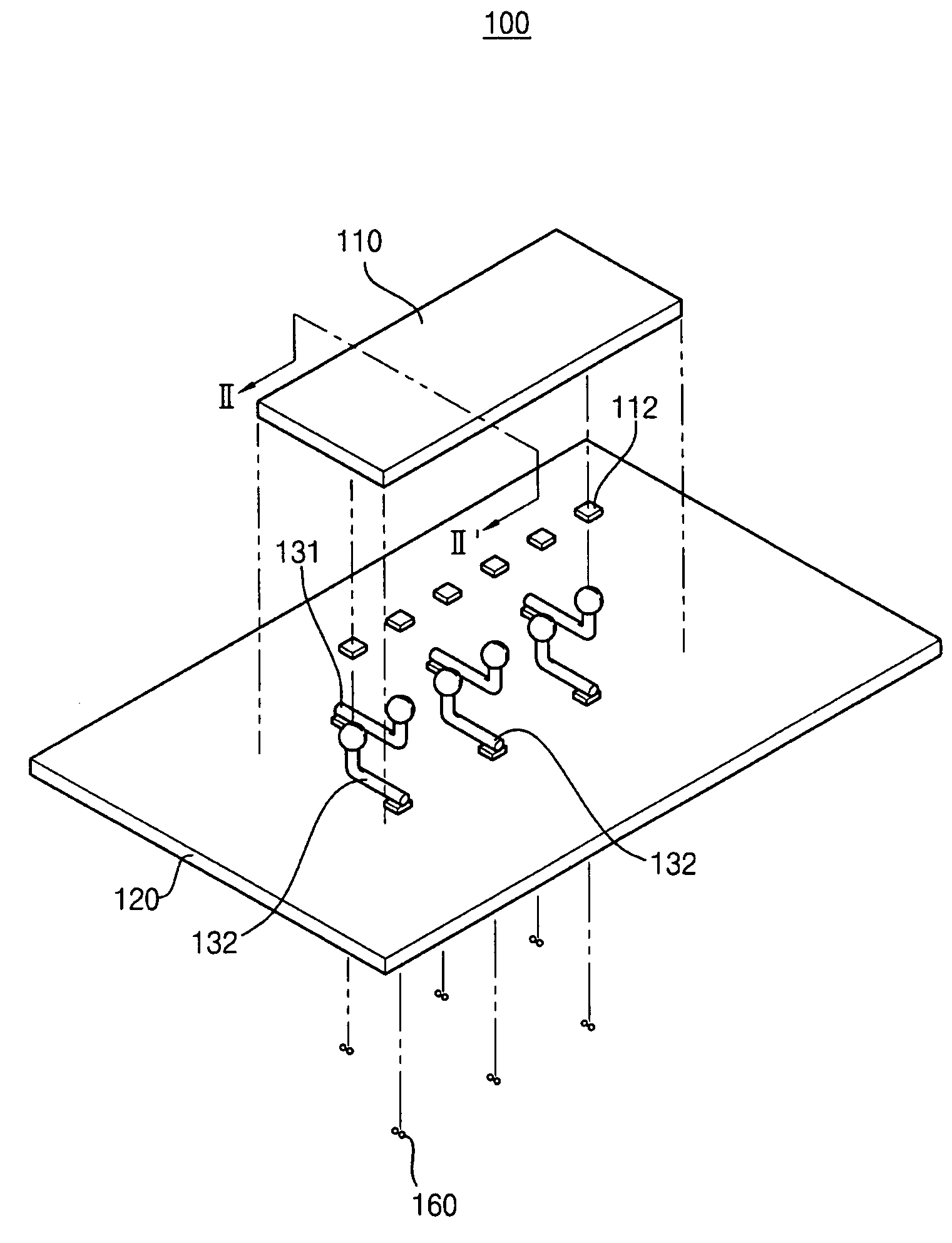
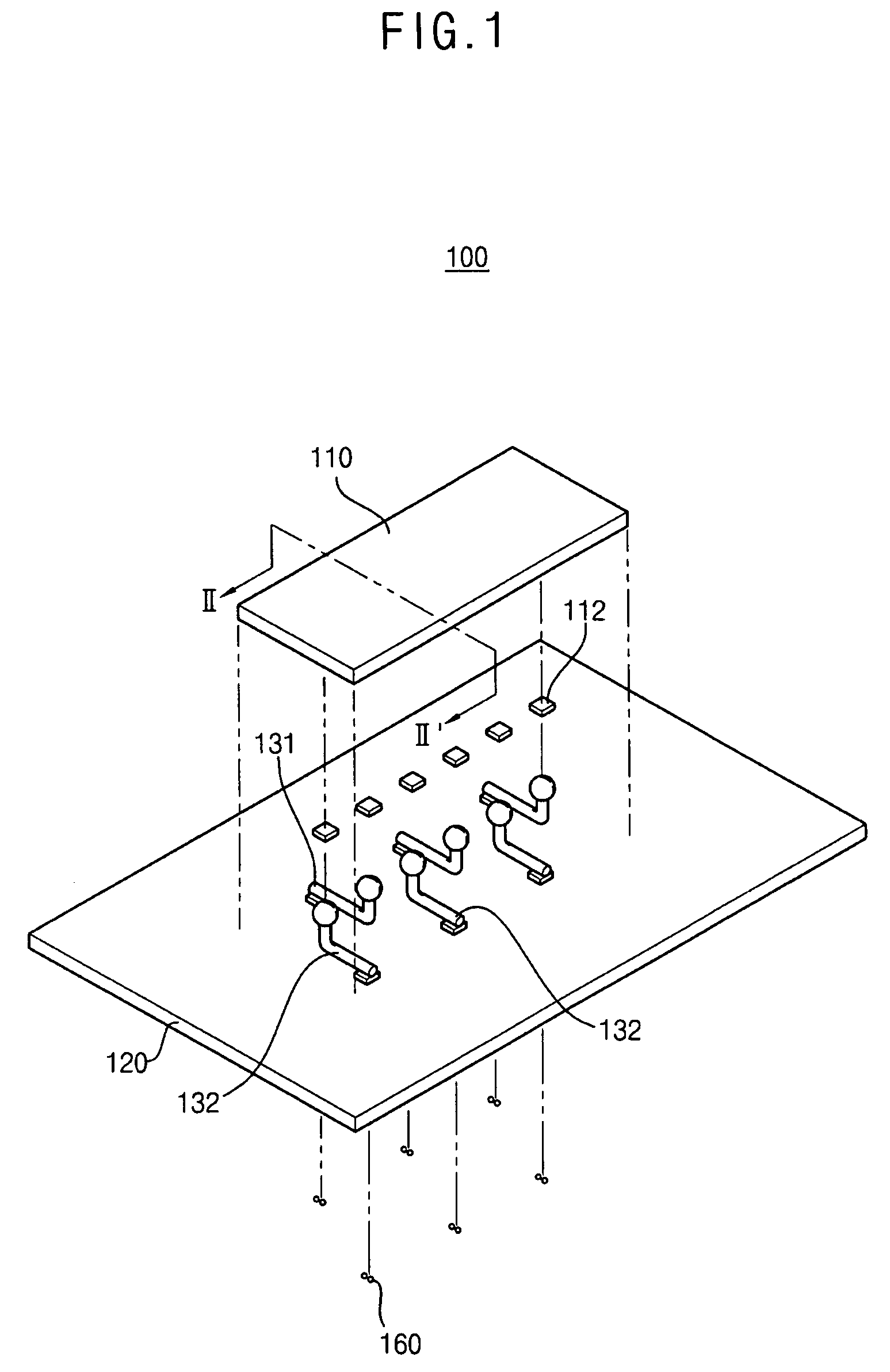
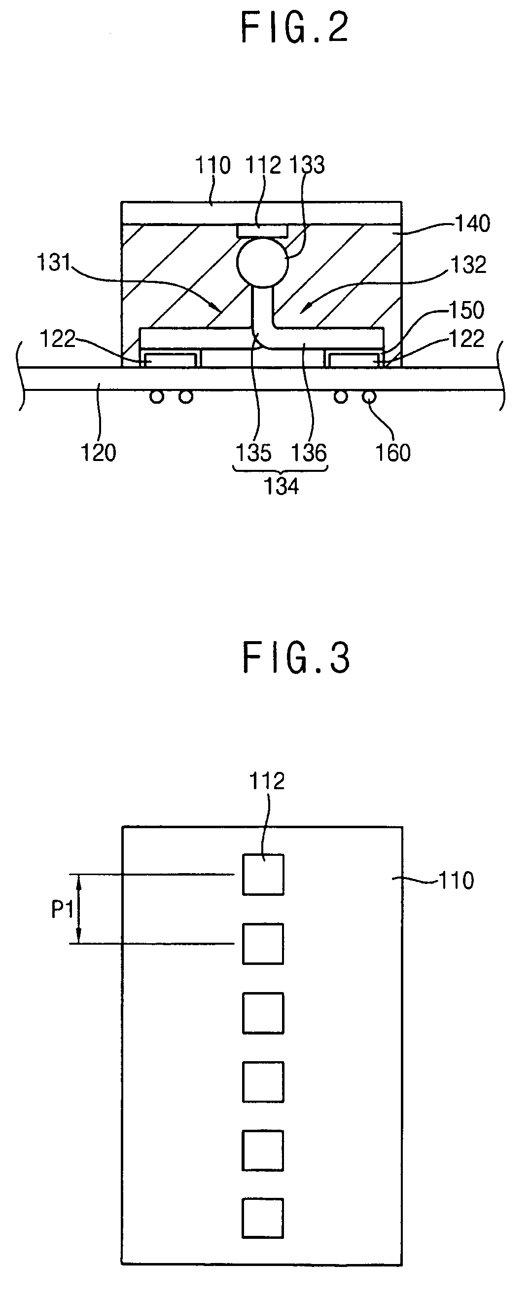
[0019]Example embodiments will now be described more fully with reference to the accompanying drawings. Embodiments, however, may be embodied in many different forms and should not be construed as being limited to example embodiments set forth herein. Rather, these example embodiments are provided so that this disclosure will be thorough and complete, and will fully convey the scope to those skilled in the art. In the drawings, the thicknesses of layers and regions may be exaggerated for clarity.

[0020]It will be understood that when an element or layer is referred to as being “on,”“connected to,”“electrically connected to,” or “coupled to” another component, it may be directly on, connected to, electrically connected to, or coupled to the other component or intervening components may be present. In contrast, when a component is referred to as being “directly on,”“directly connected to,”“directly electrically connected to,” or “directly coupled to” another component, there are no int...


PUM


Abstract

A flip-chip package may include: a semiconductor chip having first pads arranged substantially along a first direction; a substrate having second pads, arranged substantially in a zigzag form aligned with the first pads as a center line, and facing the semiconductor chip; and conductive bumps for electrically connecting the first pads to the second pads in a one-to-one relationship. Adjacent conductive bumps may extend in different directions. A method of manufacturing a flip-chip package may include: forming conductive bumps that extend along different directions on first pads of a semiconductor chip; and connecting second pads of a substrate to the conductive bumps in a one-to-one relationship. A method of manufacturing a flip-chip package may include: forming conductive bumps that extend along different directions on second pads of a substrate; and connecting first pads of a semiconductor chip to the conductive bumps in a one-to-one relationship.

Description

PRIORITY STATEMENT[0001]This application claims priority from Korean Patent Application No. 10-2006-0137916, filed on Dec. 29, 2006, in the Korean Intellectual Property Office (KIPO), the entire contents of which are incorporated herein by reference.BACKGROUND[0002]1. Field[0003]Example embodiments relate to flip-chip packages and methods of manufacturing the same. Also, example embodiments relate to flip-chip packages having a structure where a semiconductor chip faces a substrate, and methods of manufacturing the same.[0004]2. Description of Related Art[0005]Generally, a plurality of semiconductor chips may be formed by performing various semiconductor processes on a semiconductor substrate. Next, in order to mount the semiconductor chips on a printed circuit board (PCB), a semiconductor package may be formed by performing a packaging process on the semiconductor substrate. Conventional examples of the semiconductor package are disclosed in U.S. Pat. No. 5,897,326, Japanese Patent...

Claims


Application Information

Patent Timeline
Patent Type & Authority Patents(United States)
IPC IPC(8): H01L23/48
CPCH01L21/563H01L23/49811H01L23/49838H01L24/06H01L24/13H01L24/14H01L24/16H01L24/17H01L24/81H01L2224/0401H01L2224/04042H01L2224/06136H01L2224/13016H01L2224/13099H01L2224/73203H01L2224/81191H01L2224/81192H01L2224/81194H01L2224/81801H01L2924/014H01L2924/01033H01L2224/16105H01L2224/81193H01L23/02
Inventor PARK, CHAN
Owner SAMSUNG ELECTRONICS CO LTD
Why Eureka
Try Eureka