
System and method for testing a large memory area during processor design verification and validation

a technology for processor design and memory area, applied in the field of system and method for testing a large memory area during processor design verification and validation, can solve the problem of requiring a large amount of build tim

Inactive Publication Date: 2011-08-02
INT BUSINESS MASCH CORP
View PDF80 Cites 15 Cited by
  • Summary
  • Abstract
  • Description
  • Claims
  • Application Information

AI Technical Summary

Benefits of technology

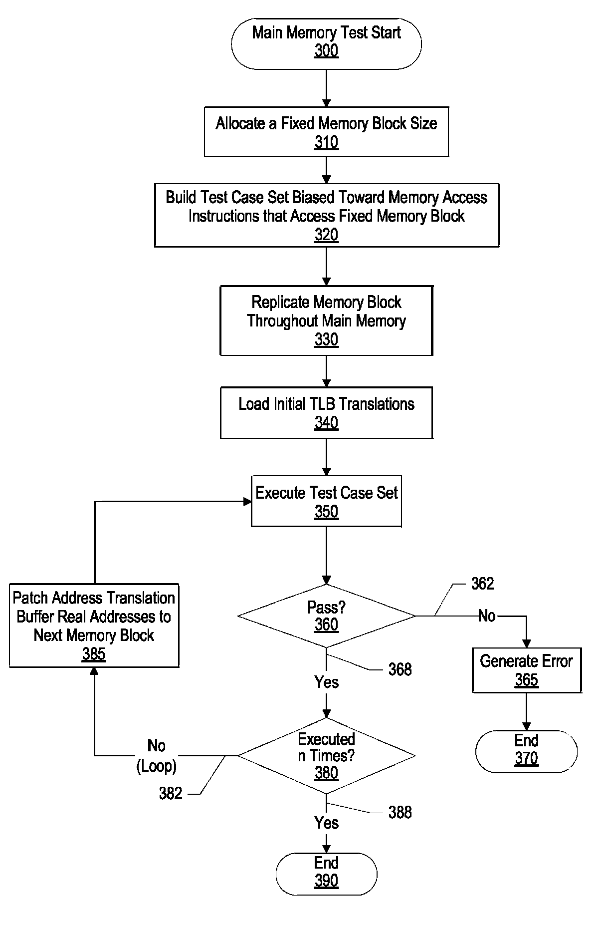
The patent describes a system and method for testing the main memory of a computer chip. The system creates a set of test cases that reference a fixed memory block and then replicates that block throughout the main memory. After each test case, the system modifies the real addresses in a translation lookaside buffer to reference the next memory block. This process allows the chip to fully test each memory block. The technical effect of this invention is to provide a more efficient and effective way to test the main memory of a computer chip.

Problems solved by technology

A challenge found is that with an increasing demand for memory, processors reside on boards that include a large amount of memory.
As a result, a large number of test cases are required to cover large memory areas, which requires a large amount of build time.

Method used


Image

  • System and method for testing a large memory area during processor design verification and validation
  • System and method for testing a large memory area during processor design verification and validation
  • System and method for testing a large memory area during processor design verification and validation

Examples


Embodiment Construction

[0024]The following is intended to provide a detailed description of an example of the invention and should not be taken to be limiting of the invention itself. Rather, any number of variations may fall within the scope of the invention, which is defined in the claims following the description.

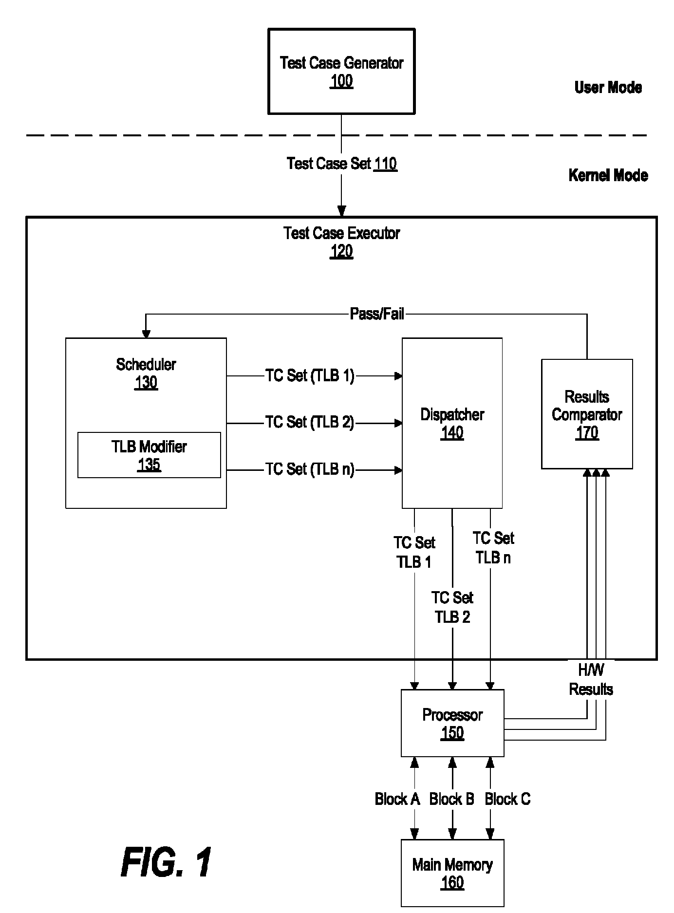
[0025]FIG. 1 is a diagram showing a test case executor re-scheduling and re-dispatching a test case set with different address translations in order to fully test a large external memory area (main memory 160). By using the same test case set and modifying the address translations, a system tester spends less time generating test cases, which allows more time to test processor 150 and main memory 160.

[0026]Test case generator 100 operates in a user mode and allocates a fixed memory block size (e.g., 64 KB) to build a test case set to test main memory 160. Test case generator 100 then builds a test case set that is biased toward memory access instructions that access an initial memory block who...


PUM


Abstract

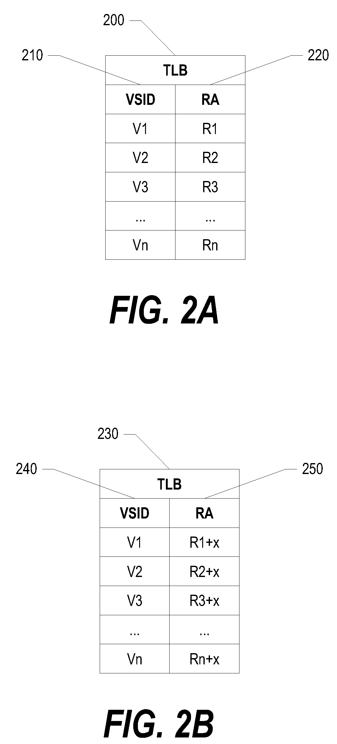
A system and method for replicating a memory block throughout a main memory and modifying real addresses within an address translation buffer to reference the replicated memory blocks during test case set re-executions in order to fully test the main memory is presented. A test case generator generates a test case set (multiple test cases) along with an initial address translation buffer that includes real addresses that reference an initial memory block. A test case executor modifies the real addresses after each test case set re-execution in order for a processor to test each replicated memory block included in the main memory.

Description

BACKGROUND OF THE INVENTION[0001]1. Technical Field[0002]The present invention relates to a system and method for testing a large memory area during processor design verification and validation. More particularly, the present invention relates to a system and method for replicating a memory block throughout a main memory and modifying real addresses within a translation lookaside buffer (TLB) to reference the replicated memory blocks during test case set re-executions in order to fully test the main memory.[0003]2. Description of the Related Art[0004]Processor testing tools exist whose goal is to generate the most stressful test case for a processor. In theory, the generated test case should provide maximum test coverage and should be interesting enough to stress various timing scenarios on the processor. The whole technology of these tools sits in the logic of building these test cases.[0005]Verifying and validating a processor using test cases typically includes three stages, whic...

Claims


Application Information

Patent Timeline
Patent Type & Authority Patents(United States)
IPC IPC(8): G11C29/00G06F11/00
CPCG06F11/263G11C2029/0401
Inventor ANVEKAR, DIVYA SUBBARAOCHOUDHURY, SHUBHODEEP ROYDUSANAPUDI, MANOJHATTI, SUNIL SURESHKAPOOR, SHAKTI
Owner INT BUSINESS MASCH CORP
Learn More