Plasma processing method, plasma processing apparatus and storage medium
a plasma processing and plasma technology, applied in the field of micro lens formation, can solve the problems of reducing the sensitivity of the solid state imaging device, etc., and achieve the effect of large surface area
- Summary
- Abstract
- Description
- Claims
- Application Information
AI Technical Summary
Benefits of technology
Problems solved by technology
Method used
Image


Examples
experiment 1
Initial Evaluation
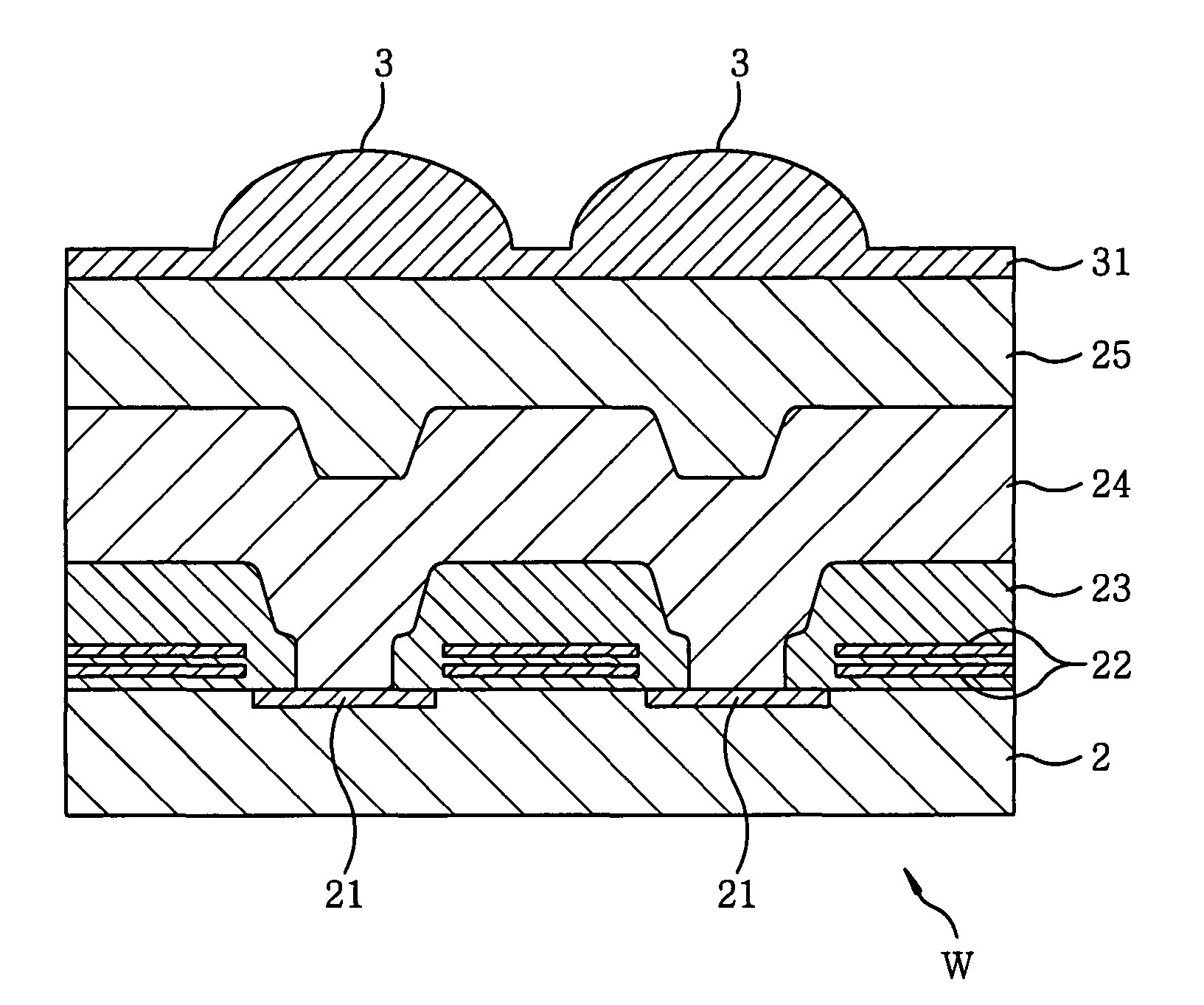
[0070]Etching was performed on the wafer W shown in FIG. 2A under the following processing conditions, to thereby form micro lenses 3:[0071]frequency of the high frequency power supply 63: 13.56 MHz;[0072]electric power of the high frequency power supply 63: specified separately;[0073]processing pressure: 5.3 Pa (40 mTorr);[0074]processing gas: CF4 / C4F8=100 / 10 sccm;[0075]temperature of the wafer W: 30° C.; and[0076]processing time: etching was performed until 1.25 μm of the transcription film 31 was etched and immediately thereafter, the etching was stepped.
example 1-1
[0077]In the above processing conditions, the electric power of the high frequency power supply 63 was set to be 1400 W.
example 1-2
[0078]In the above processing conditions, the electric power of the high frequency power supply 63 was set to be 2000 W.
PUM
| Property | Measurement | Unit |
|---|---|---|
| diagonal distance D2 | aaaaa | aaaaa |
| diagonal distance D2 | aaaaa | aaaaa |
| temperature | aaaaa | aaaaa |
Abstract
Description
Claims
Application Information
 - R&D
- Intellectual Property
- Life Sciences
- Materials
- Tech Scout
- Unparalleled Data Quality
- Higher Quality Content
- 60% Fewer Hallucinations
Browse by: Latest US Patents, China's latest patents, Technical Efficacy Thesaurus, Application Domain, Technology Topic, Popular Technical Reports.
© 2025 PatSnap. All rights reserved.Legal|Privacy policy|Modern Slavery Act Transparency Statement|Sitemap|About US| Contact US: help@patsnap.com