Logic cell array and bus system

a logic cell array and bus system technology, applied in logic circuits, program control, multi-processor architectures, etc., can solve problems such as system problems, system failures, and large number of cells having to communicate with each other, and achieve optimal chip form and easy linking of data

a logic cell array and bus system technology, applied in logic circuits, program control, multi-processor architectures, etc., can solve problems such as system problems, system failures, and large number of cells having to communicate with each other, and achieve optimal chip form and easy linking of data

US8058899B2Inactive Publication Date: 2011-11-15SCIENTIA SOL MENTIS AG

Image

  • Logic cell array and bus system
  • Logic cell array and bus system
  • Logic cell array and bus system

Examples


Embodiment Construction

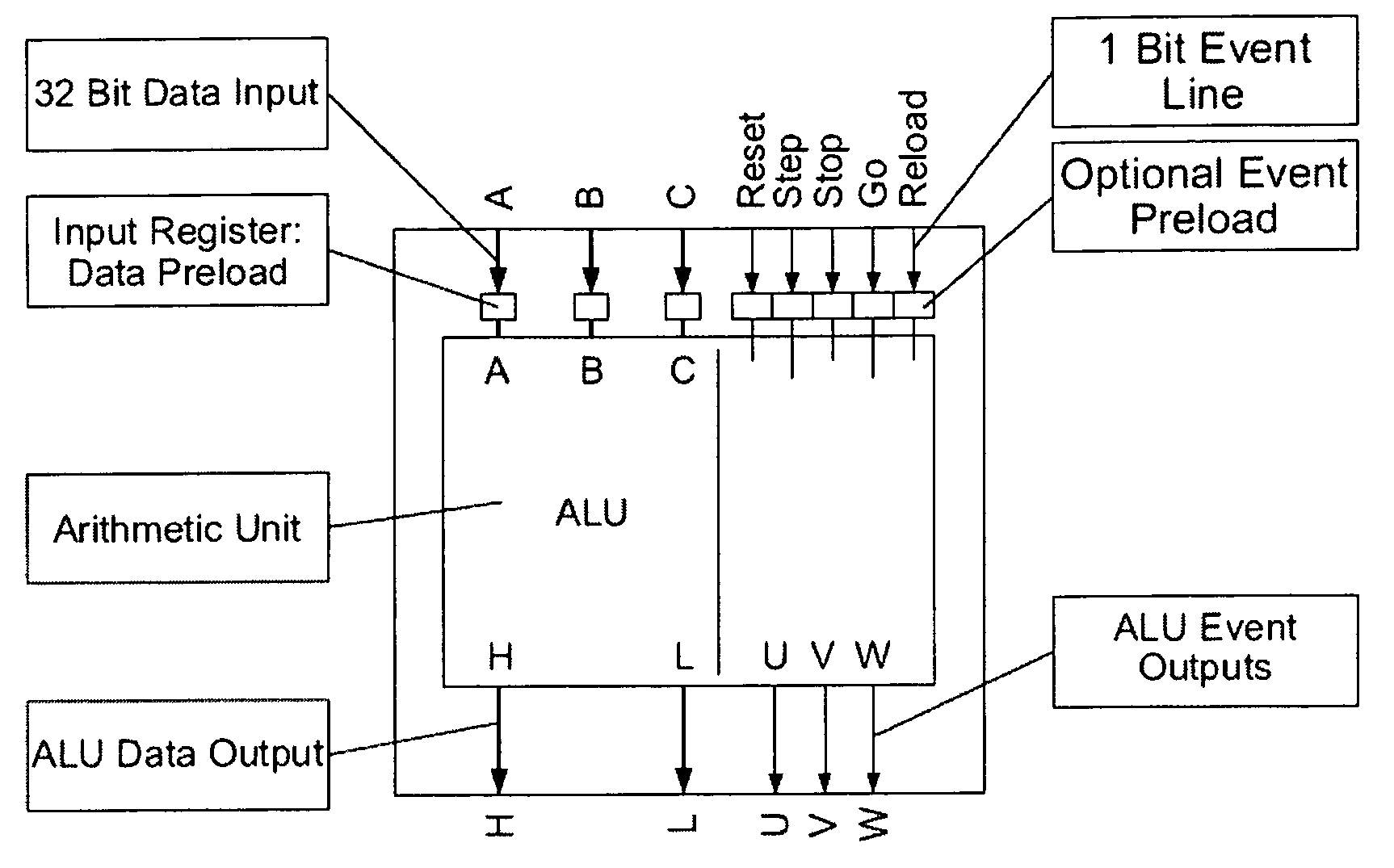
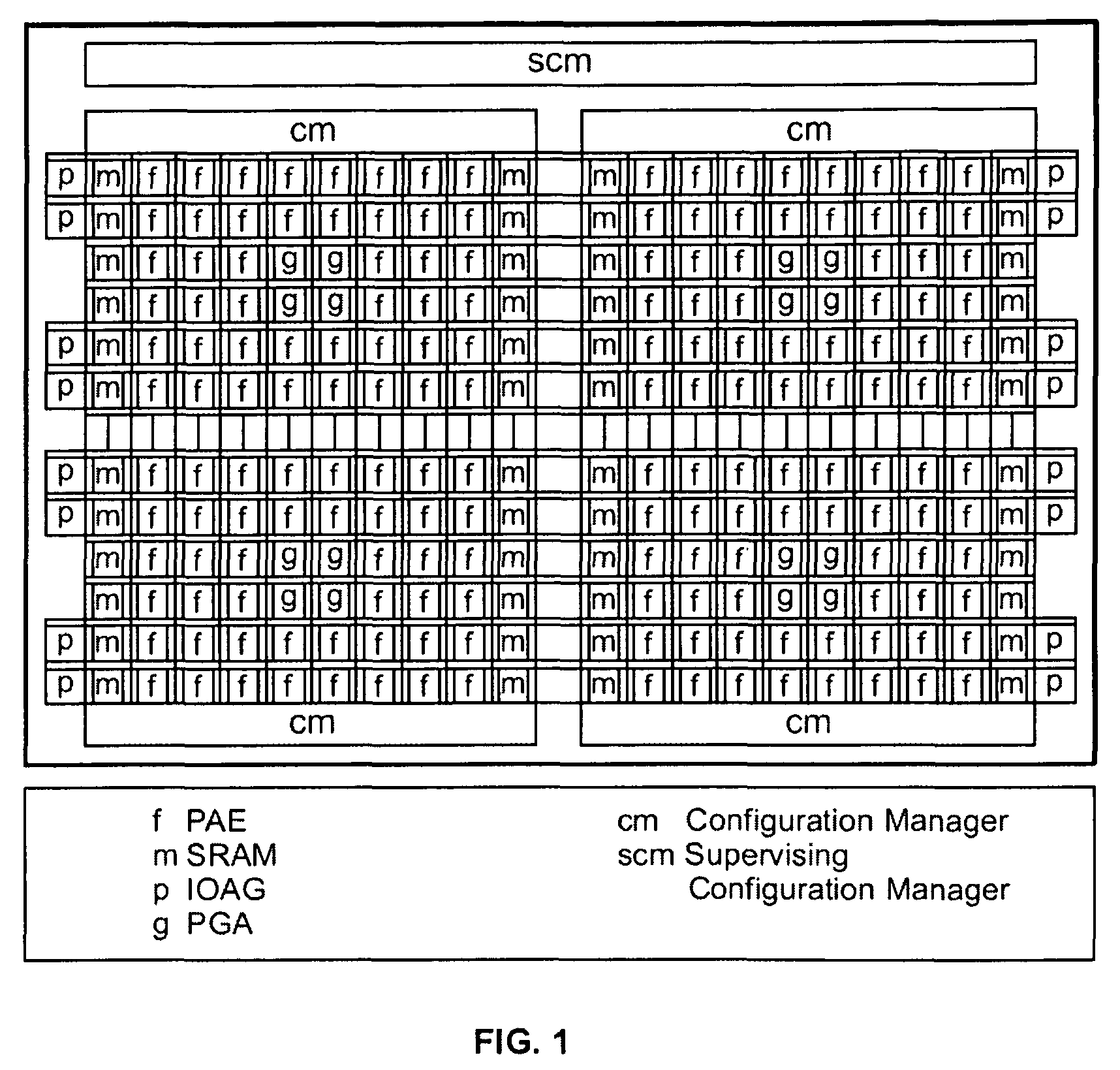
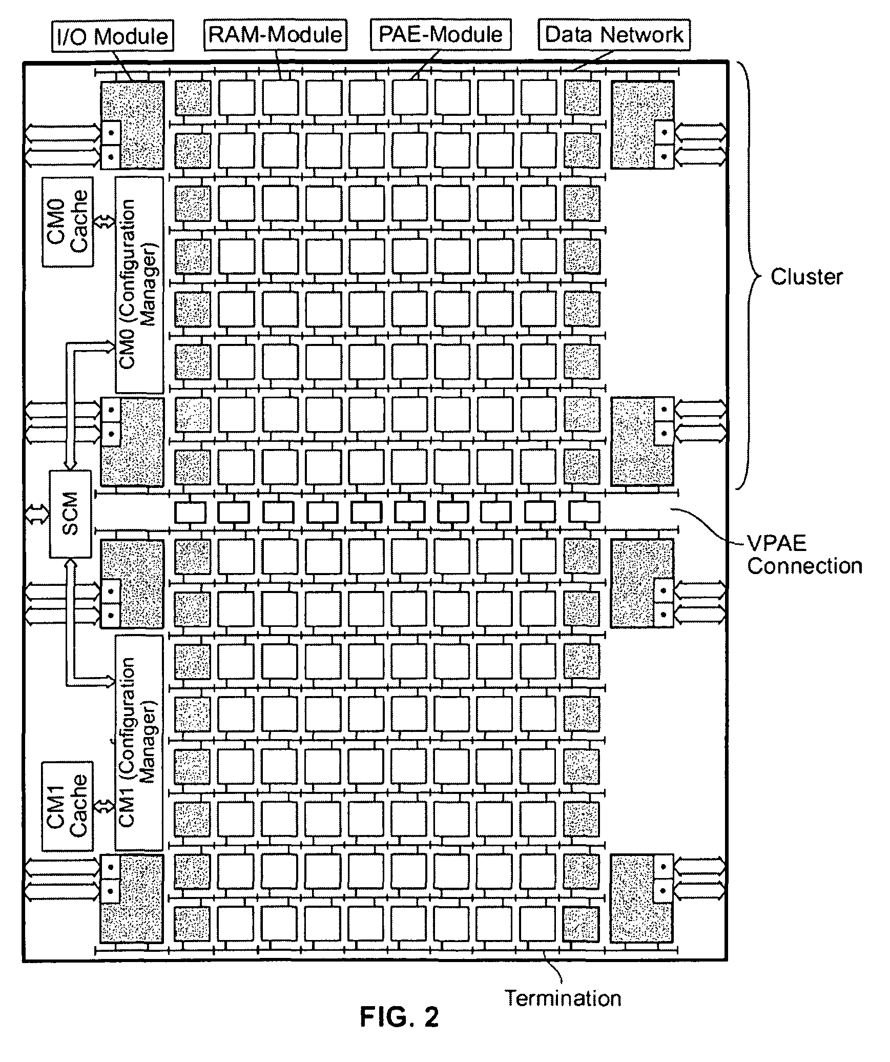
[0064]According to FIG. 1, a processor 1, which may form a unit that may be characterized as an XPP (extreme processing platform), includes two fields or clusters including: a number of arithmetic logic cells (ALU-PAE's=arithmetic logic unit processing array element); memory cells (RAM-PAE's=Random Access Memory processing array element); several illustrated as four input / output cells (I / O elements, input / output processing array element); a bus system running through each field; and a configuration manager that is assigned to the field, these elements together as a cluster forming a unit, which by itself is capable of processing data and doing so as a reconfigurable unit and a higher-order configuration manager being assigned to the two configuration managers (CM) of the cluster in order to form thereby a master cluster or the XPP. It is possible using tree-like hierarchical structures to have more than two fields of processor elements cooperate. In this manner, a higher-order confi...


PUM


Abstract

A logic cell array having a number of logic cells and a segmented bus system for logic cell communication, the bus system including different segment lines having shorter and longer segments for connecting two points in order to be able to minimize the number of bus elements traversed between separate communication start and end points.

Description

CROSS REFERENCE TO RELATED APPLICATIONS[0001]This application is a continuation of and claims priority to U.S. patent application Ser. No. 10 / 398,546, filed on Jan. 20, 2004, now U.S. Pat. No. 7,595,659 and claims benefit of and priority to International Application Serial No. PCT / EP01 / 11593, filed on Oct. 8, 2001, which claims benefit of and priority to U.S. Patent Application Ser. No. 60 / 238,855, filed on Oct. 6, 2000, the entire contents of each of which are expressly incorporated herein by reference.FIELD OF THE INVENTION[0002]The present invention relates to logic cell arrays.BACKGROUND INFORMATION[0003]Logic cell arrays, such as, for example, reconfigurable logic cell arrays include, as particular types, systolic arrays, neuronal networks, multi-processor systems, processors having a number of arithmetic-logic units, and / or logic cells and / or communicative / peripheral cells (I / O), networking and / or network chips, such as crossbar switches, as well as FPGA, DPGA, Xputer, Chamele...

Claims


Application Information

Patent Timeline
15 Nov 2011
Publication
US8058899B2
IPC
H03K19/177; G06F7/52; G06F15/78
CPC
G06F15/7867; G06F15/8023; G06F13/4027; Y02D10/00; G06F9/3001; G06F13/4022; G06F15/7825; G06F15/80
Inventors
VORBACH, MARTIN; MAY, FRANK