Method of programming nonvolatile memory device

a nonvolatile memory and programming technology, applied in the field of nonvolatile memory devices, can solve problems such as failure to achieve ideal threshold voltage distribution, and achieve the effect of minimizing the interference effect of neighboring cells

Active Publication Date: 2012-01-31
SK HYNIX INC
View PDF5 Cites 9 Cited by
  • Summary
  • Abstract
  • Description
  • Claims
  • Application Information

AI Technical Summary

Benefits of technology

[0011]One or more embodiments relate to a method of programming a nonvolatile memory device, which is capable of minimizing the effect of interference on neighboring cells while program operations are performed in a nonvolatile memory device having MLCs.

Problems solved by technology

Accordingly, while the logical pages are programmed, neighboring memory cells are continuously subject to interference, which leads to a failure in an ideal threshold voltage distribution.

Method used


Image

  • Method of programming nonvolatile memory device
  • Method of programming nonvolatile memory device
  • Method of programming nonvolatile memory device

Examples


Embodiment Construction

[0027]Hereinafter, some embodiments of the present disclosure will be described in detail with reference to the accompanying drawings. The figures are provided to allow those having ordinary skill in the art to understand the scope of the embodiments of the disclosure.

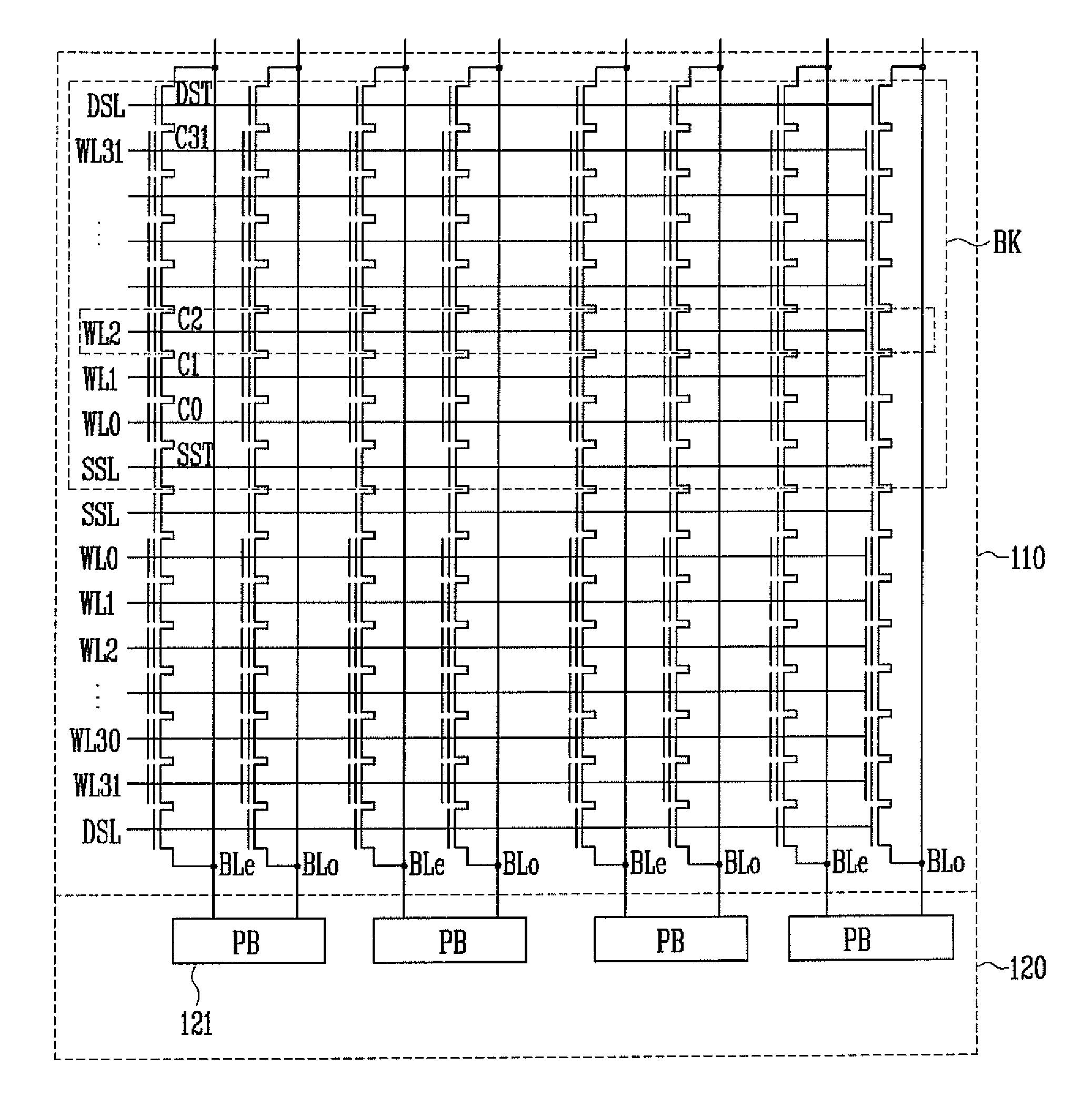
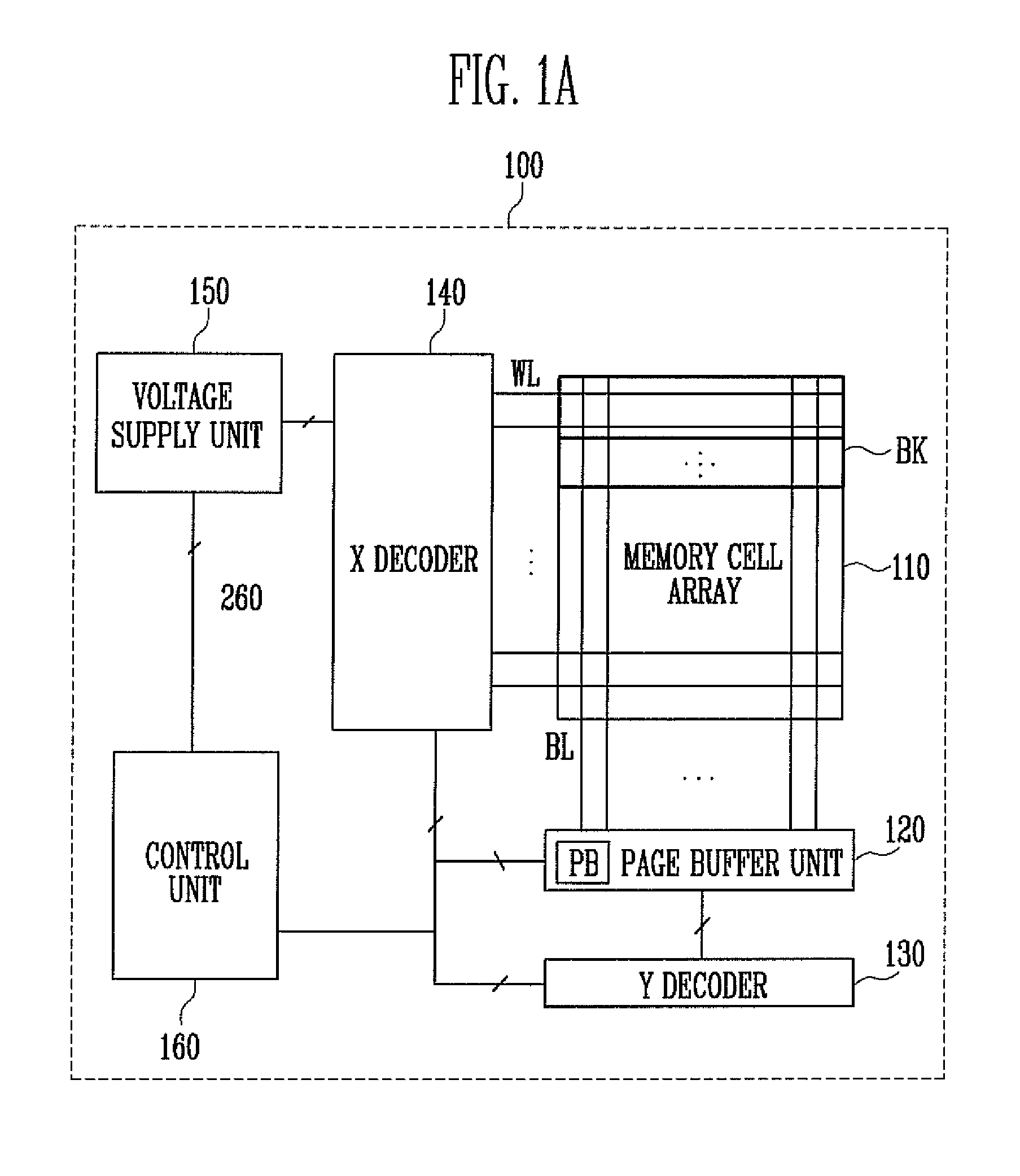
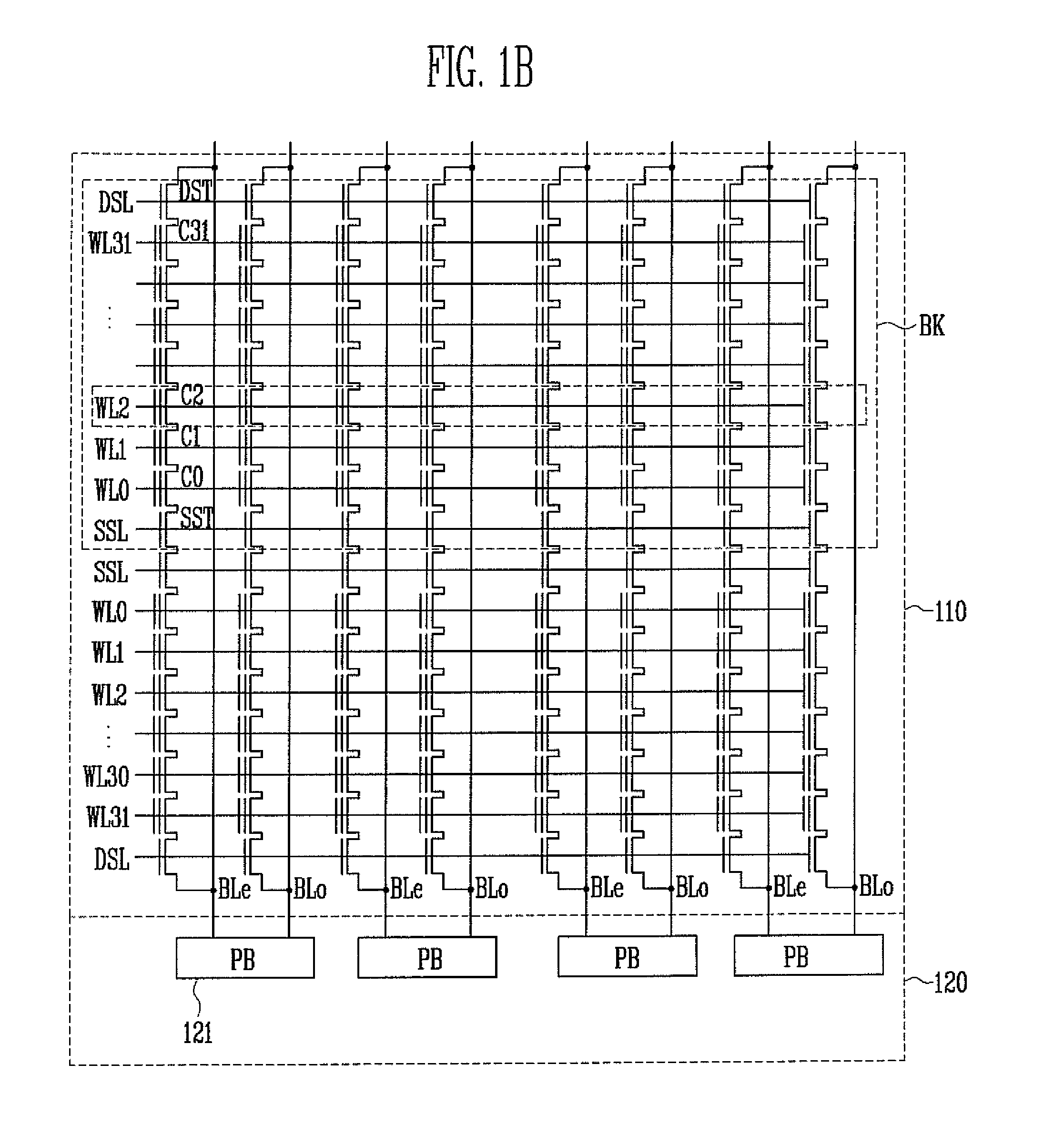
[0028]FIG. 1A is a diagram showing a nonvolatile memory device according to an embodiment of this disclosure.

[0029]Referring to FIG. 1A, the nonvolatile memory device 100 according to the embodiment of this disclosure includes a memory cell array 110, a page buffer unit 120, a Y decoder 130, an X decoder 140, a voltage supply unit 150, and a control unit 160.

[0030]The memory cell array 110 includes a number of memory blocks BK. The memory blocks each include memory cells each capable of storing 3-bit information. Furthermore, the memory cells are coupled together by word lines WL and bit lines BL.

[0031]The page buffer unit 120 includes a number of page buffers PB. Each of the page buffers PB are coupled to one or more ...


PUM


Abstract

A method of programming a nonvolatile memory device includes sequentially programming first to (n−1)th logical pages of all the physical pages of a first memory block of the memory blocks in response to a first program command, a step of loading data of the first to (n−1)th logical pages stored in a first physical page of the first memory block and latching the loaded data in first to (n−1)th latches of each of the page buffers, respectively, when receiving a second program command after programming all the first to (n−1)th logical pages, and latching new program data, received along with the second program command, in an nth latch of the corresponding page buffer and programming the data, stored in the first to nth latches of the page buffer, into a first physical page of a second memory block of the memory blocks.

Description

CROSS-REFERENCE TO RELATED APPLICATION[0001]Priority to Korean patent application number 10-2009-0008801 filed on Feb. 4, 2009, the entire disclosure of which is incorporated by reference herein, is claimed.BACKGROUND[0002]One or more embodiments relate to a method of programming a nonvolatile memory device and, more particularly, to a method of programming a nonvolatile memory device, which is capable of storing 3-bit information.[0003]A nonvolatile memory device has the advantages of random access memory (RAM), which enables the writing and erasure of data, and read only memory (ROM), which retains data even without the supply of power, and so has recently been widely used for the storage media of portable electronic devices, such as digital cameras, personal digital assistants (PDAs), and MP3 players.[0004]The nonvolatile memory device includes a memory cell array, a row decoder, a page buffer unit, etc. The memory cell array includes a plurality of word lines elongated in rows, ...

Claims


Application Information

Patent Timeline
Patent Type & Authority Patents(United States)
IPC IPC(8): G11C16/04
CPCG11C11/5628G11C16/0483G11C16/3418G11C16/06G11C16/34
Inventor JUNG, MIN JOONG
Owner SK HYNIX INC
Why Eureka
Try Eureka