Optical scanning device

a scanning device and optical technology, applied in the field of optical scanning devices, can solve the problems of insufficient correction of errors in the angle of reflection surfaces of polygon mirrors, loss of conjugate relation, and increase of sub-scanning magnification, etc., and achieve good balance

Active Publication Date: 2012-06-19
KONICA MINOLTA BUSINESS TECH INC
View PDF11 Cites 3 Cited by
  • Summary
  • Abstract
  • Description
  • Claims
  • Application Information

AI Technical Summary

Benefits of technology

[0007]In view of the above problems, an object of the present invention is to provide an optical scanning device that is capable of achieving a good balance between focusing of a light beam onto a photoreceptor surface and correction to errors in the angle of reflecting surfaces of a polygon mirror by using an over-filled optical system.

Problems solved by technology

However, when an over-filled optical system is used, a converging point in the vicinity of a polygon mirror of a light beam that has passed through a light source optical system may be displaced from reflecting surfaces of the polygon mirror depending on the angle of view, due to movement of the reflecting surfaces along with rotations of a polygon mirror.
Therefore, there has been a problem that the light beam is focused onto a point displaced from the photoreceptor surface if the reflecting surfaces and the photoreceptor surface are maintained in conjugation, and conversely, if the preference is given to focusing the light beam onto the photoreceptor surface, the conjugate relation is lost, and errors in the angle of reflecting surfaces of the polygon mirror cannot be corrected adequately.
In particular, in attempting to downsize the device, a sub-scanning magnification is increased, and it is impossible to correct both errors in the angle of reflecting surfaces and errors in the sub-scanning-direction image surface at the same time.

Method used


Image

  • Optical scanning device
  • Optical scanning device
  • Optical scanning device

Examples


first embodiment

See FIGS. 2 to 9

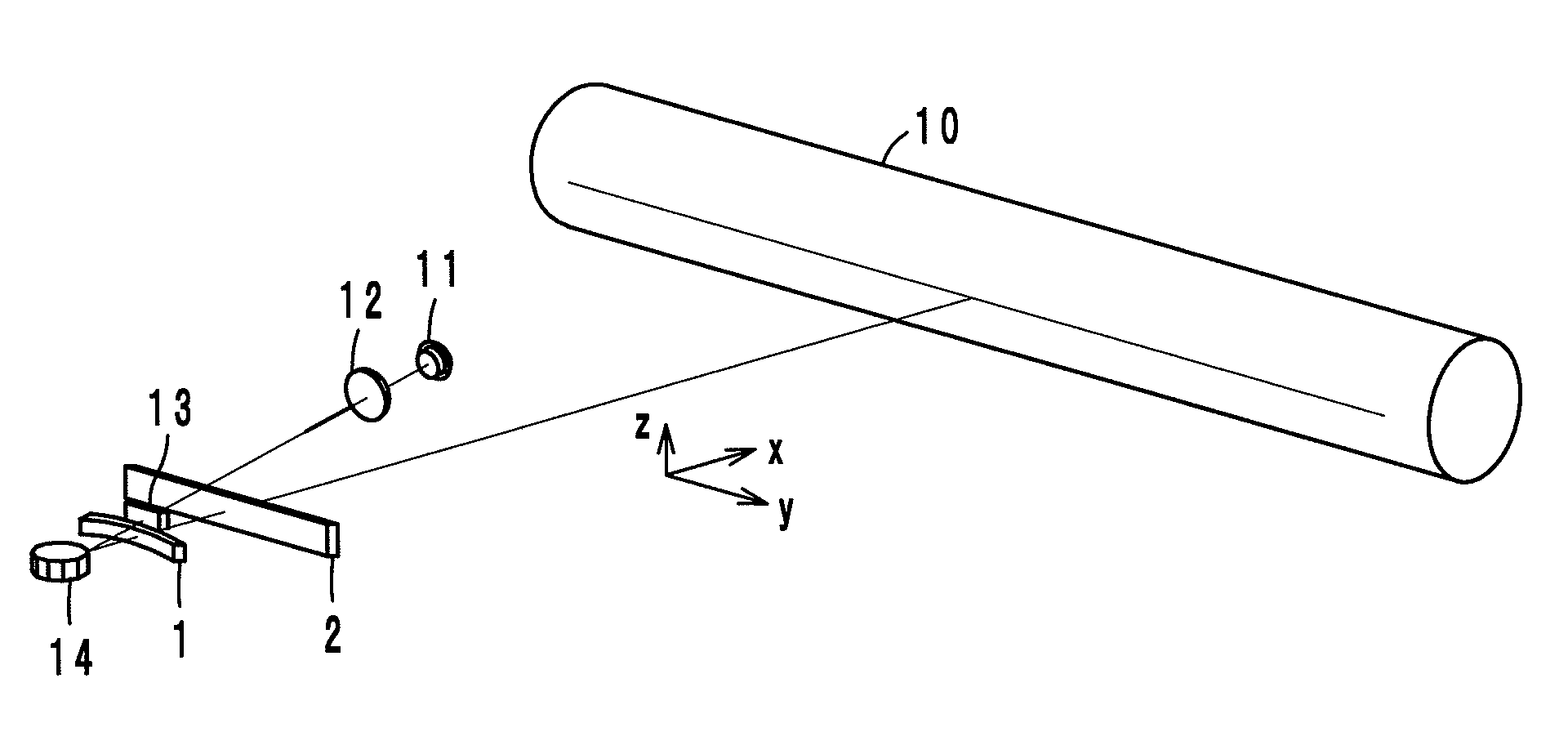
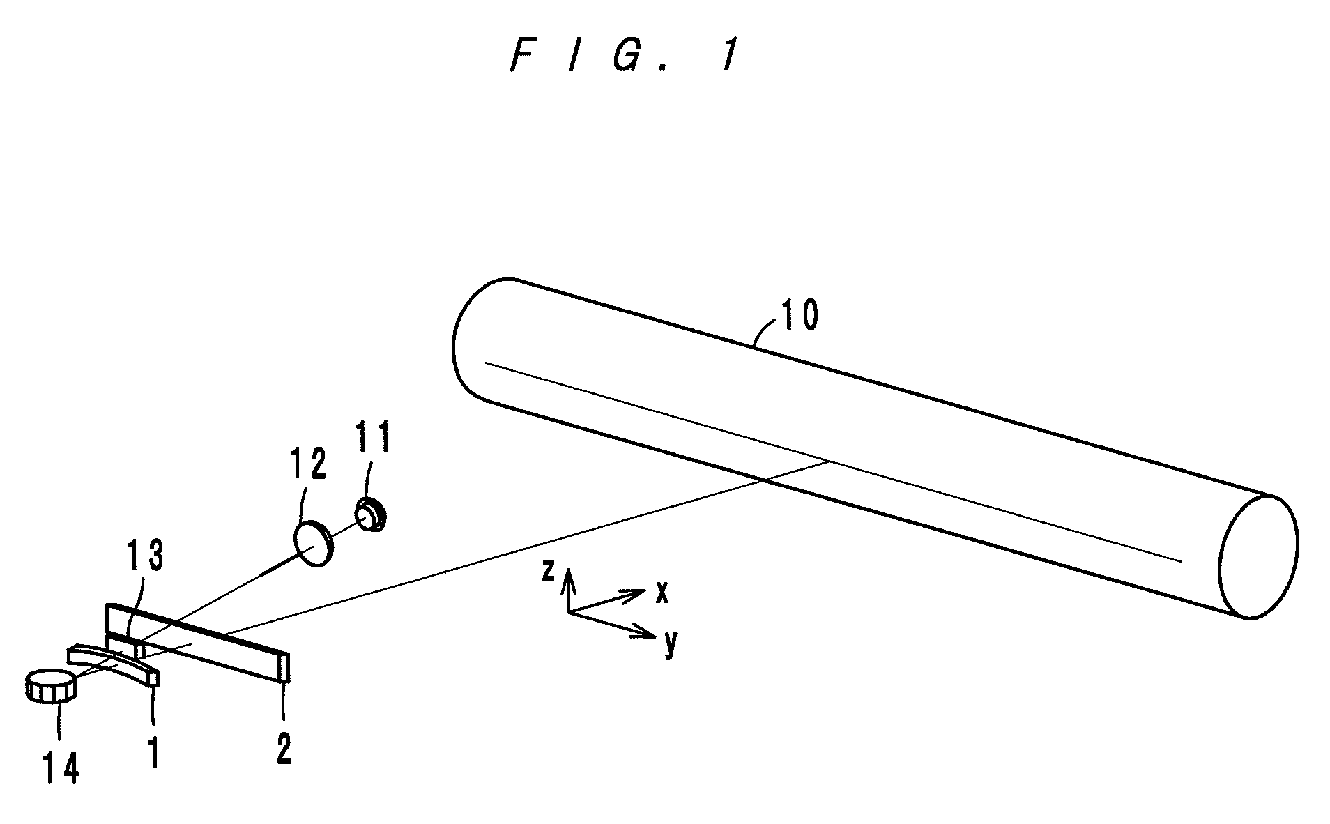
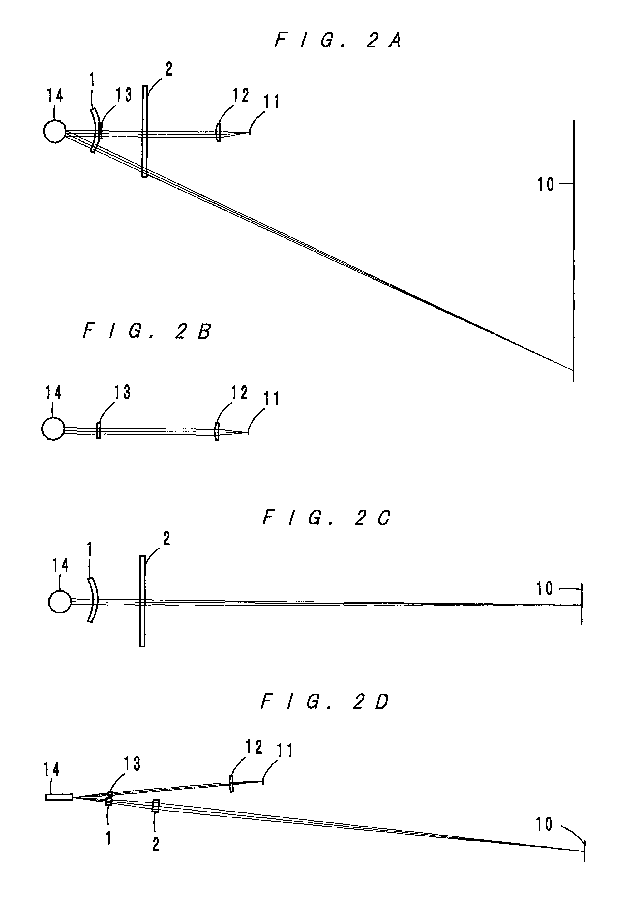
[0037]An optical scanning device according to a first embodiment, as shown in FIG. 2A to FIG. 2D, comprises a laser diode 11, a collimator lens 12, a free-form-surface lens 13, a polygon mirror 14 and scanning lenses 1 and 2. A light beam B1 incident to the reflecting surfaces of the polygon mirror 14 is wider in the main-scanning direction y than a single reflecting surface 14a of the polygon mirror 14 (see FIG. 3A and FIG. 3B), and the width of a light beam used for image writing is regulated by the reflecting surface 14a. In FIG. 2A to FIG. 2D, it is drawn that the light beam B1 in an upstream side has the same width as that after the regulation. As is apparent from comparison of FIG. 2A and FIG. 2B, the portion of the free-form-surface lens 13 through which a light beam B2 used for image writing passes changes as a deflection angle changes.

[0038]FIG. 3A and FIG. 3B show the light beam B2 reflected on the polygon mirror 14, and a light beam B3 that is not used for...

second embodiment

See FIGS. 10 to FIG. 14

[0062]As shown in FIG. 10, an optical scanning according to a second embodiment is basically of a similar structure to that of the first embodiment. The optical scanning device according to the second embodiment generally comprises a laser diode 11 as a light source, a collimator lens 12, a free-form-surface lens 13, a polygon mirror 14 having a plurality of flat reflecting surfaces, and scanning lenses 1 and 2. The second embodiment is different from the first embodiment in that the scanning lenses 1 and 2 are disposed slightly farther from the polygon mirror 14. Further, effects of the second embodiment are basically the same as those of the first embodiment.

[0063]Table 4, Table 5, and Table 6 below show construction data that numerically represents the second embodiment. Although the positional relation among the optical elements in the second embodiment is different from that in the first embodiment, the types of the surfaces, the positioning order of the ...

third embodiment

See FIGS. 15 to 19

[0069]As shown in FIG. 15, an optical scanning according to a third embodiment is basically of a similar structure to that of the first embodiment. The optical scanning device according to the third embodiment generally comprises a laser diode 11 as a light source, a collimator lens 12, a free-form-surface lens 13, a polygon mirror 14 having a plurality of flat reflecting surfaces, and scanning lenses 1 and 2. The third embodiment is different from the first embodiment in that the scanning lenses 1 and 2 are disposed slightly closer to the polygon mirror 14. Further, effects of the third embodiment are basically the same as those of the first embodiment.

[0070]Table 7, Table 8, and Table 9 below show construction data that numerically represents the third embodiment. Although the positional relation among the optical elements in the third embodiment is different from that in the first embodiment, the types of the surfaces, the positioning order of the optical elemen...


PUM


Abstract

An optical scanning device having: a light source for emitting a light beam; a deflector having a plurality of flat reflecting surfaces; a first optical system disposed between the light source and the deflector; and a second optical system disposed between the deflector and a photoreceptor surface, and configured such that the reflecting surfaces of the deflector and the photoreceptor surface are conjugated in a sub-scanning direction at every deflection angle in a main-scanning range. In the optical scanning device, the light beam traveling from the first optical system to the deflector has a width greater than a dimension in a main-scanning direction of each reflecting surface of the deflector, and the light beam passes through different portions of the first optical system depending on whether the light beam is to be deflected by the deflector to be directed to an edge portion of the main-scanning range or to be directed to a center portion of the main-scanning range such that the light beam traveling to the deflector has a smaller average wavefront curvature in a sub-scanning direction when the light beam is to be deflected by the deflector to be directed to an edge portion of the main-scanning range than when the light beam is to be deflected by the deflector to be directed to the center portion of the main-scanning range.

Description

[0001]This application is based on Japanese Patent Application No. 2010-148850 filed on Jun. 30, 2010, the content of which is incorporated herein by reference.BACKGROUND OF THE INVENTION[0002]1. Field of the Invention[0003]The present invention relates to an optical scanning device, in particular, to an optical scanning device for irradiating a photoreceptor with light to form an electrostatic latent image.[0004]2. Description of Related Art[0005]There has conventionally been proposed a technique for downsizing an optical scanning device by using an over-filled optical system with a high scanning efficiency to cancel aberrations of a scanning optical system with aberrations of a light source optical system, as described in Japanese Patent Laid-Open Publication No. 2001-208995, for example.[0006]However, when an over-filled optical system is used, a converging point in the vicinity of a polygon mirror of a light beam that has passed through a light source optical system may be displ...

Claims


Application Information

Patent Timeline
Patent Type & Authority Patents(United States)
IPC IPC(8): G02B26/08
CPCG02B26/125
Inventor INAGAKI, YOSHIHIRO
Owner KONICA MINOLTA BUSINESS TECH INC
Why Eureka
Try Eureka