Schottky diode with improved high current behavior

a high current behavior, schottky technology, applied in the direction of basic electric elements, electrical apparatus, semiconductor devices, etc., can solve problems such as diode destruction, and achieve the effect of improving potential homogenisation

Inactive Publication Date: 2013-09-03
ERIS TECH CORP
View PDF17 Cites 0 Cited by
  • Summary
  • Abstract
  • Description
  • Claims
  • Application Information

AI Technical Summary

Benefits of technology

[0003]The object of the invention is to increase the reverse current strength of Schottky barrier diodes of the general type while at the same time minimising the forward voltage drop by means of a suitable construction. It is irrelevant whether they are Schottky diodes on an n-conducting or p-conducting epitaxial layer. Furthermore, the embodiment according to the invention is applicable to all semiconductor materials and crystal orientations which are considered for Schottky diodes.DESCRIPTION OF THE INVENTION

Problems solved by technology

In the event that an applied reverse surge voltage exceeds the protected voltage range, an avalanche breakdown takes place in the guard ring area of the arrangement, which can lead to destruction of the diode.

Method used


Image

  • Schottky diode with improved high current behavior
  • Schottky diode with improved high current behavior
  • Schottky diode with improved high current behavior

Examples


Embodiment Construction

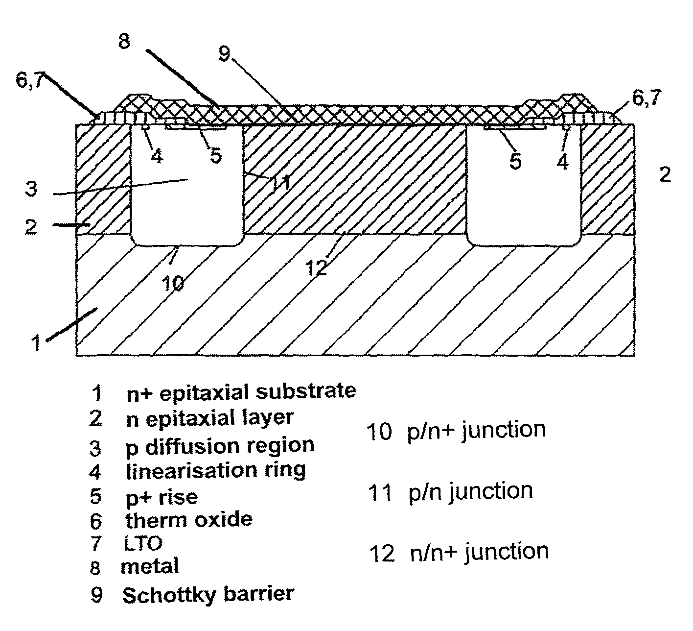
[0004]The structure according to the invention of the arrangement is explained below using FIG. 2. A significant stabilisation of the high current behaviour with minimisation of the forward voltage drop at the same time is achieved according to the invention in that, in the diffusion region (3) of the second doping type, a more highly doped region of the same conductivity mode (5) is introduced in such a manner that the region of the first conductivity mode (2) which is covered by the barrier metal silicide (9) and the second conductivity mode (3) are connected in a conductive manner. The region (3) of the second conductivity mode is diffused in such a manner that it reaches the more highly doped region (1) of the first conductivity mode (1), with at the same time an outward diffusion of the dopand taking place in the direction of the semiconductor surface from the more highly doped substrate layer (1) into the more weakly doped layer (2) of the same conductivity mode. The impurity ...


PUM


Abstract

In the diffusion region (3) of the second conductivity mode, a more highly doped region of the same conductivity mode (5) is introduced in such a manner that the region of the first conductivity mode (2) which is covered by the metal silicide (9) and of the second conductivity mode (3) are connected in a conductive manner. The region (3) of the second conductivity mode is diffused in such a manner that it reaches the more highly doped region (1) of the first doping type (1), with an outward diffusion of the doping from the more highly doped substrate layer (1) into the more weakly doped layer (2) of the same conductivity mode in the direction of the semiconductor surface taking place at the same time.

Description

FIELD OF APPLICATION OF THE INVENTION[0001]The invention relates to a semiconductor component with a Schottky barrier junction and the production thereof. The invention in particular relates to the improvement of the voltage strength in reverse mode and surge current strength in forward mode while at the same time reducing the forward voltage drop compared to conventional embodiments. A method for producing the construction is specified.KNOWN TECHNICAL SOLUTIONS[0002]Schottky diodes are rectifying semiconductor arrangements which consist of a weakly doped semiconductor layer (2) of a first doping and a metal layer which is deposited thereon, with the direct junction layer from the semiconductor to the metal being known as a Schottky contact. The typical details of a Schottky diode are shown in the U.S. Pat. No. 4,206,540. In the German patent DE 199 39 484 is the description of a typical guard ring construction. FIG. 1 shows such an arrangement schematically. For improved current yi...

Claims


Application Information

Patent Timeline
Patent Type & Authority Patents(United States)
IPC IPC(8): H01L29/872
CPCH01L29/66143H01L29/872H01L29/861
Inventor RESCHKE, MICHAELHILLEMANN, HANS-JURGENGUNTHER, KLAUS
Owner ERIS TECH CORP
Why Eureka
Try Eureka