Solar cell array with isotype-heterojunction diode

a solar cell and junction diode technology, applied in the direction of pv power plants, light radiation electric generators, generators/motors, etc., can solve the problems of reduced solar cell efficiencies, reduced production yields, and limited solar cell voltage and electrical current output, so as to minimize the forward voltage drop and minimize the effect of power dissipation

Inactive Publication Date: 2010-02-09
THE BOEING CO
View PDF5 Cites 6 Cited by
  • Summary
  • Abstract
  • Description
  • Claims
  • Application Information

AI Technical Summary

Benefits of technology

[0006]The present invention provides a solar cell with an integrated isotype heterojunction diode construction in which the diode is grown into the same monolithic structure as the active photovoltaic structure of the solar cell. The diode minimizes the forward voltage drop while preserving low currents under reverse bias, with the result that power dissipation is minimized. The isotype heterojunction diode is a majority carrier device, which is less sensitive to defects produced by charged particle radiation in a space environment than is a minority carrier device. Solar cells using the present approach and operated on spacecraft are therefore more stable over time in their operating performance, as compared with solar cells protected by other types of diode structures.
[0008]The isotype heterojunction diode comprises a basic diode unit where an interface, specifically a hetero-interface, is formed between two semiconductor layers of different compositions but having the same dopant character (i.e., both layers are either doped negatively or doped positively, but may not be doped oppositely). An asymmetry in current flow, or rectification, may be generated across this hetero-interface by an offset or a step in energy between the two layers. This energy step is termed a band offset and results from the difference in energy between the conduction band edges or the valence band edges for the two layers. The band edges that align to produce a significant band offset, viz., many times the thermal background energy, may be used to form the isotype heterojunction. When the energy step is favorable for rectification at the band offset between the conduction band edges of the two layers, then the dopant character will be negative and permit rectification in the flow of electrons. When the energy step is favorable at the band offset between the valence band edges of the two layers, then the dopant character will be positive and permit rectification in the flow of holes. Either electron flow or hole flow can be used to rectify the current passing between the layers. Furthermore, these band offsets may be generated at both Type-1 (where ΔEV, the valence band offset, and ΔEC, the conduction band offset, are displaced in voltage in opposite directions, and the electrons and holes are confined in the same layer) and Type-2 (where ΔEV and ΔEC are displaced in voltage in the same direction, and the electrons and holes are confined in different layers) hetero-interfaces so long as the dopant character conforms to the condition just mentioned at the conduction and valence band offsets. A third layer that is a semiconductor or a metal may be added to help reduce overall series resistance.
[0013]The present approach provides a solar cell array in which each solar cell is protected against damage from imposed reverse current flows by an electrically parallel bypass diode that is integrated into the structure of each solar cell. The isotype heterojunction diode is a majority carrier device, and therefore is relatively insensitive to the defects produced by charged particle radiation found in a space environment. The isotype heterojunction diode has a capacitance that is smaller than many other types of diodes with comparable current-voltage characteristics. The isotype heterojunction diode minimizes the forward voltage drop while preserving low currents under reverse bias, with the result that the power dissipation is minimized.

Problems solved by technology

The voltage and electrical current output of the solar cell are limited by the materials of construction and the surface area of the solar cell.
This approach requires the bonding of the interconnection taps and the leads, a time-consuming process when a large number of solar cells are present in the solar cell circuit.
The available approaches are complex and cause assembly difficulties as well as reduced production yields and reduced solar cell efficiencies.
This approach is also complex, and has reduced production yields and reduced solar cell efficiency.

Method used


Image

  • Solar cell array with isotype-heterojunction diode
  • Solar cell array with isotype-heterojunction diode
  • Solar cell array with isotype-heterojunction diode

Examples


Embodiment Construction

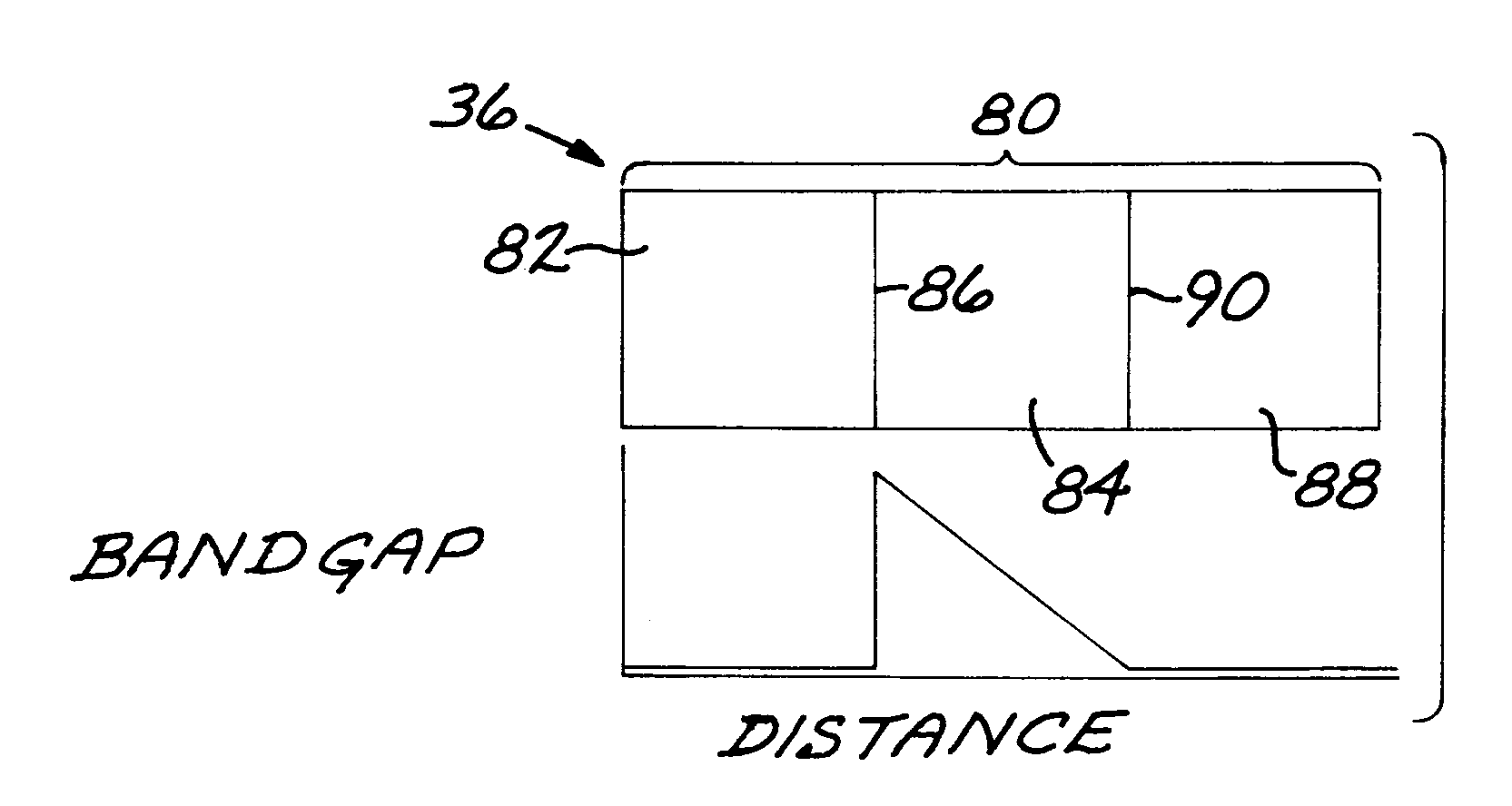
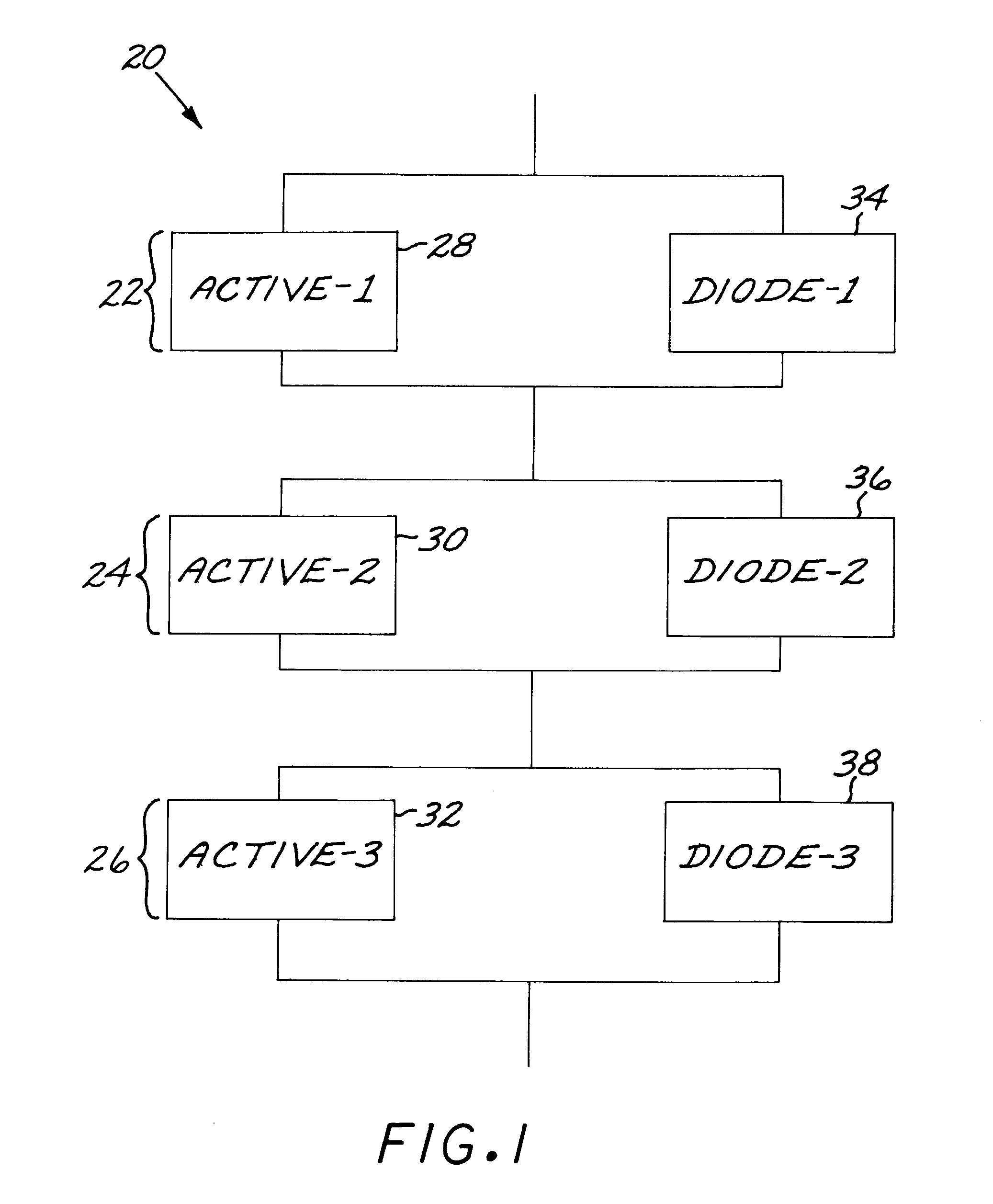
[0021]FIG. 1 depicts a solar cell array 20 having at least one solar cell, and in this case three solar cells 22, 24, and 26. The solar cells 22, 24, and 26 are electrically connected in series. Each solar cell 22, 24, and 26 includes an active region, respectively 28, 30, and 32, which produces a photovoltaic output when illuminated, and a isotype heterojunction diode, respectively 34, 36, and 38, electrically connected in parallel with the respective active region 28, 30, and 32. If one of the active regions, for example, active region 30, should cease to produce an electrical output, the current impressed on the active region 30, in the absence of its respective diode 36, by the other series-connected solar cells 22 and 26 would damage the solar cell 24. The isotype heterojunction diode 36 provides a parallel current path around the active region 30 to protect it from such damage.

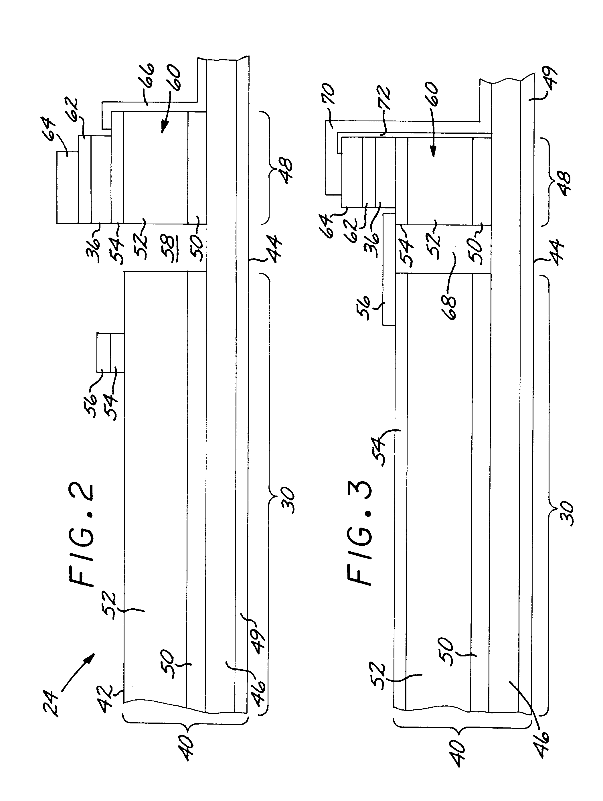
[0022]FIG. 2 illustrates an exemplary one of the solar cells 24, in which the active region 30 and th...


PUM


Abstract

A solar cell array has at least one solar cell including a photovoltaic structure having a sun-facing front face and a back face, and having an active region, and an isotype heterojunction diode connected in electrical parallel with the active region of the photovoltaic structure.

Description

[0001]This invention relates to solar cells and more particularly to a solar cell with an integral diode to protect the solar cell from damage in reverse-bias conditions.BACKGROUND OF THE INVENTION[0002]A solar cell is formed of two semiconductor layers in facing contact with each other at a semiconductor junction. When illuminated by the sun or other light source, the solar cell produces a voltage between the semiconductor layers. Advanced solar cells may include more than two semiconductor layers and their respective pairwise semiconductor junctions. The various pairs of semiconductor layers of the advanced solar cells form subcells, with each subcell tuned to a specific spectral component of the sun to maximize the power output. The voltage and electrical current output of the solar cell are limited by the materials of construction and the surface area of the solar cell. Most commonly, a number of subcells are electrically interconnected in series to form a solar cell structure t...

Claims


Application Information

Patent Timeline
Patent Type & Authority Patents(United States)
IPC IPC(8): H01L31/00H01L25/00H01L31/042H02N6/00
CPCH01L27/142Y02E10/50
Inventor JOSLIN, DAVID E.FETZER, CHRISTOPHER M.
Owner THE BOEING CO
Why Eureka
Try Eureka