Insulated gate bipolar transistor and method for manufacturing the same

a technology of insulated gate bipolar transistor and manufacturing method, which is applied in the direction of basic electric elements, electrical apparatus, semiconductor devices, etc., can solve the problems of device damage, device turn-off performance may deteriorate, etc., and achieve the effect of reducing the amount of hole current, minimizing the forward voltage drop, and increasing the latch-up curren

Inactive Publication Date: 2011-08-16
DONGBU HITEK CO LTD
View PDF8 Cites 0 Cited by
  • Summary
  • Abstract
  • Description
  • Claims
  • Application Information

AI Technical Summary

Benefits of technology

[0007]Embodiments of the present invention provide an insulated gate bipolar transistor and methods for manufacturing the same, capable of inhibiting the parasitic thyristor latch-up while minimizing the forward voltage drop.
[0011]Therefore, the parasitic thyristor latch-up can be inhibited while minimizing the forward voltage drop by increasing latch-up current through reducing the amount of hole current injected into a resistance region Rp of the base, which is the cause of the latch-up.

Problems solved by technology

However, if the sum of current gains of an NPN transistor and a PNP transistor provided in an equivalent circuit is equal to or greater than 1, a PNPN thyristor is turned on, so that turn-off performance by the gate may deteriorate, which is called latch-up.
Such a latch-up may restrict an SOA (safe operation area) of the IGBT and cause over current so that devices may be damaged.

Method used


Image

  • Insulated gate bipolar transistor and method for manufacturing the same
  • Insulated gate bipolar transistor and method for manufacturing the same
  • Insulated gate bipolar transistor and method for manufacturing the same

Examples


Embodiment Construction

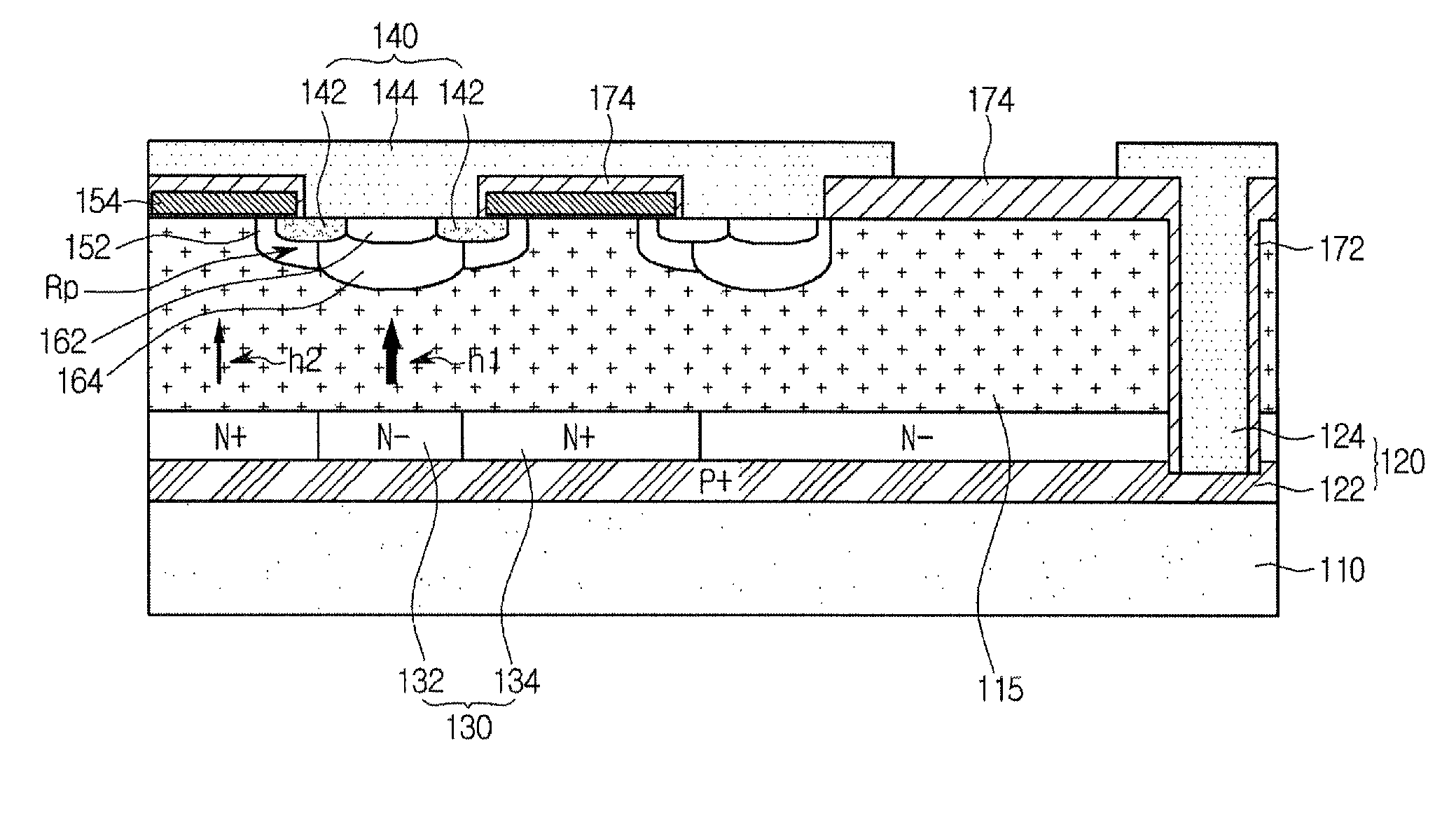
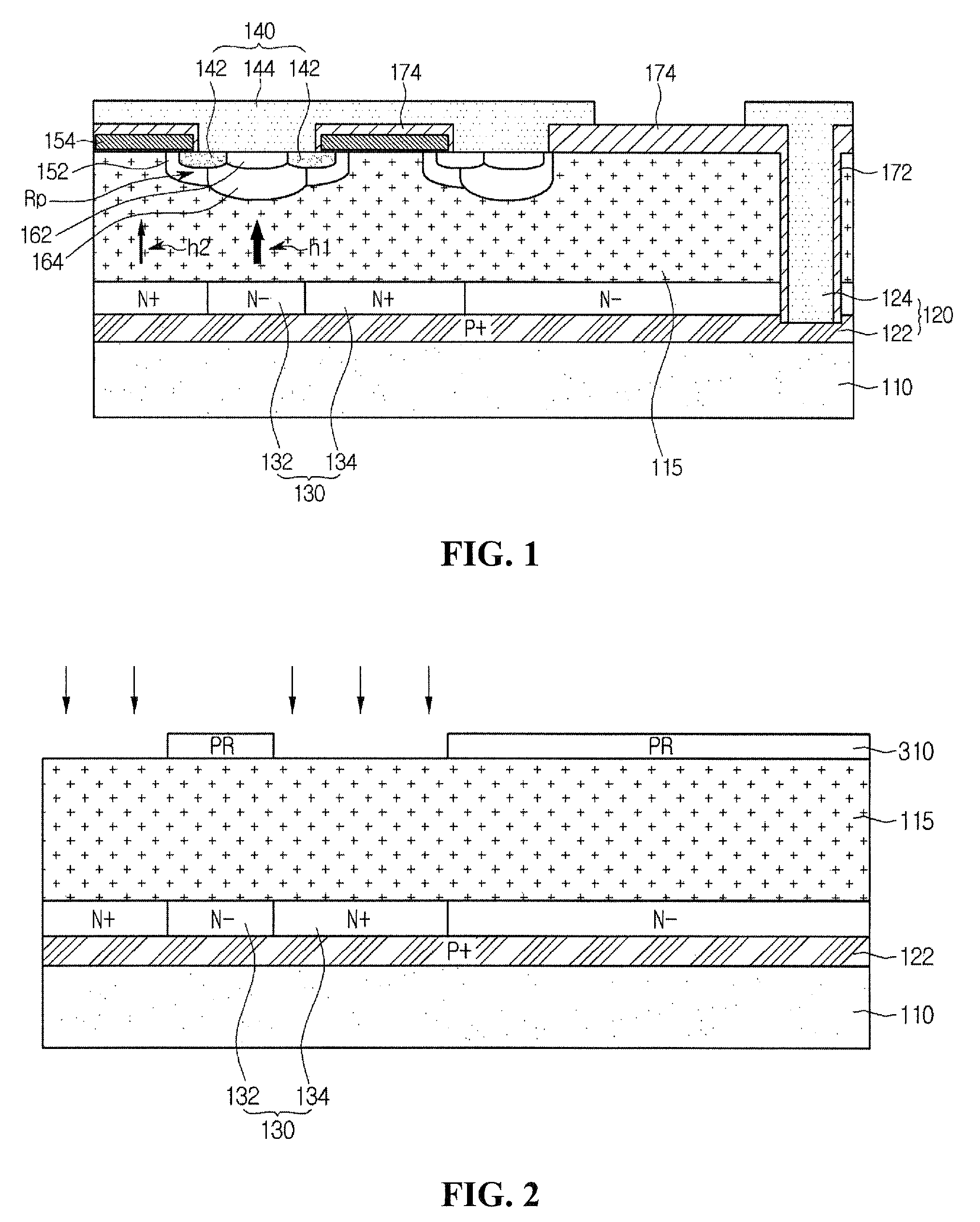
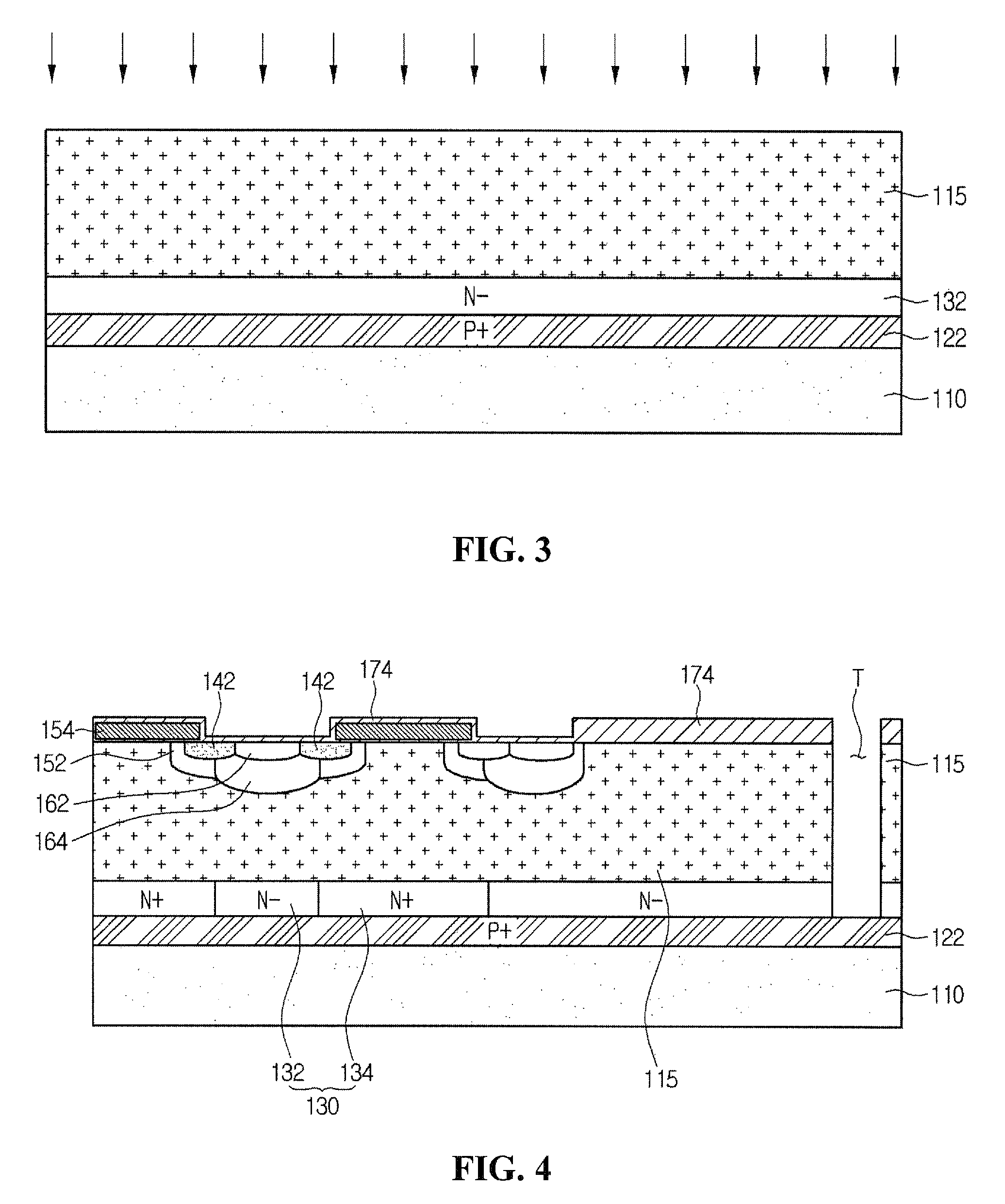
[0014]Hereinafter, embodiments of an insulated gate bipolar transistor and a method for manufacturing the same will be described in detail with reference to accompanying drawings.

[0015]When the terms “on” or “over” are used herein, when referring to layers, regions, patterns, or structures, it is understood that the layer, region, pattern or structure can be directly on another layer or structure, or intervening layers, regions, patterns, or structures may also be present. When the terms “under” or “below” are used herein, when referring to layers, regions, patterns, or structures, it is understood that the layer, region, pattern or structure can be directly under the other layer or structure, or intervening layers, regions, patterns, or structures may also be present.

[0016]Although in the following description a first conductive type is referring to a P-type and a second conductive type is referring to an N-type, embodiments are not limited thereto.

[0017]FIG. 1 is a cross-sectional...


PUM


Abstract

An insulated gate bipolar transistor according to an embodiment includes a first conductive type collector ion implantation area in a substrate; a second conductive type buffer layer, including a first segment buffer layer and a second segment buffer layer, on the first conductive collector ion implantation area; a first conductive type base area on the second conductive type buffer layer; a gate on the substrate at a side of the first conductive type base area; a second conductive type emitter ion implantation area in the first conductive type base area; an insulating layer on the gate; an emitter electrode electrically connected to the second conductive type emitter ion implantation area; and a collector electrode electrically connected to the first conductive collector ion implantation area. The first segment buffer layer can be aligned below a portion of the base area and can have a lower density of second conductive type ions than that of the second segment buffer layer adjacent the first segment buffer layer.

Description

CROSS-REFERENCE TO RELATED APPLICATION[0001]The present application claims the benefit under 35 U.S.C. §119 of Korean Patent Application No. 10-2007-0087562, filed Aug. 30, 2007, which is hereby incorporated by reference in its entirety.BACKGROUND[0002]An insulated gate bipolar transistor (IGBT) is a device having the advantageous characteristics of an insulated gate structure of a metal oxide semiconductor (MOS) transistor and the high current density of a bipolar transistor.[0003]In contrast to the MOS transistor, a conventional IGBT has a parasitic PNPN thyristor structure including a collector P, a drift region N, a base P and an emitter N.[0004]However, if the sum of current gains of an NPN transistor and a PNP transistor provided in an equivalent circuit is equal to or greater than 1, a PNPN thyristor is turned on, so that turn-off performance by the gate may deteriorate, which is called latch-up.[0005]Such a latch-up may restrict an SOA (safe operation area) of the IGBT and c...

Claims


Application Information

Patent Timeline
Patent Type & Authority Patents(United States)
IPC IPC(8): H01L21/331
CPCH01L29/66325H01L29/7394H01L21/18
Inventor LEE, SANG YONG
Owner DONGBU HITEK CO LTD
Why Eureka
Try Eureka