Liquid crystal display device comprising first and second data link lines electrically connected to odd and even data lines respectively and crossing each other to connect even and odd data pad electrodes respectively

a technology of liquid crystal display device and data link line, which is applied in semiconductor devices, optics, instruments, etc., can solve the problems of display degradation, afterimage, and increase of resistance of data link lin

Inactive Publication Date: 2013-09-17
LG DISPLAY CO LTD
View PDF5 Cites 4 Cited by
  • Summary
  • Abstract
  • Description
  • Claims
  • Application Information

AI Technical Summary

Benefits of technology

[0017]To reduce an area of the non-display region NAA, it is suggested to reduce areas of the data pads. This, however, causes increase of resistance of the data pad and delay of the data signal, and thus, display degradation, for example, afterimage occurs.

Problems solved by technology

This, however, causes increase of resistance of the data pad and delay of the data signal, and thus, display degradation, for example, afterimage occurs.
Alternatively, when a width CD of the data link line is reduced, this causes increase of resistance of the data link line and delay of the data signal.
As the distances are reduced, the data link lines may be subject to a short-circuit due to conductive particles, which are in a process chamber, stuck to the data link lines.
These problems make it difficult to reduce the area of the non-display region.

Method used


Image

  • Liquid crystal display device comprising first and second data link lines electrically connected to odd and even data lines respectively and crossing each other to connect even and odd data pad electrodes respectively
  • Liquid crystal display device comprising first and second data link lines electrically connected to odd and even data lines respectively and crossing each other to connect even and odd data pad electrodes respectively
  • Liquid crystal display device comprising first and second data link lines electrically connected to odd and even data lines respectively and crossing each other to connect even and odd data pad electrodes respectively

Examples


first embodiment

[0037]FIG. 3 is a plan view illustrating an array substrate of an LCD device according to the present invention.

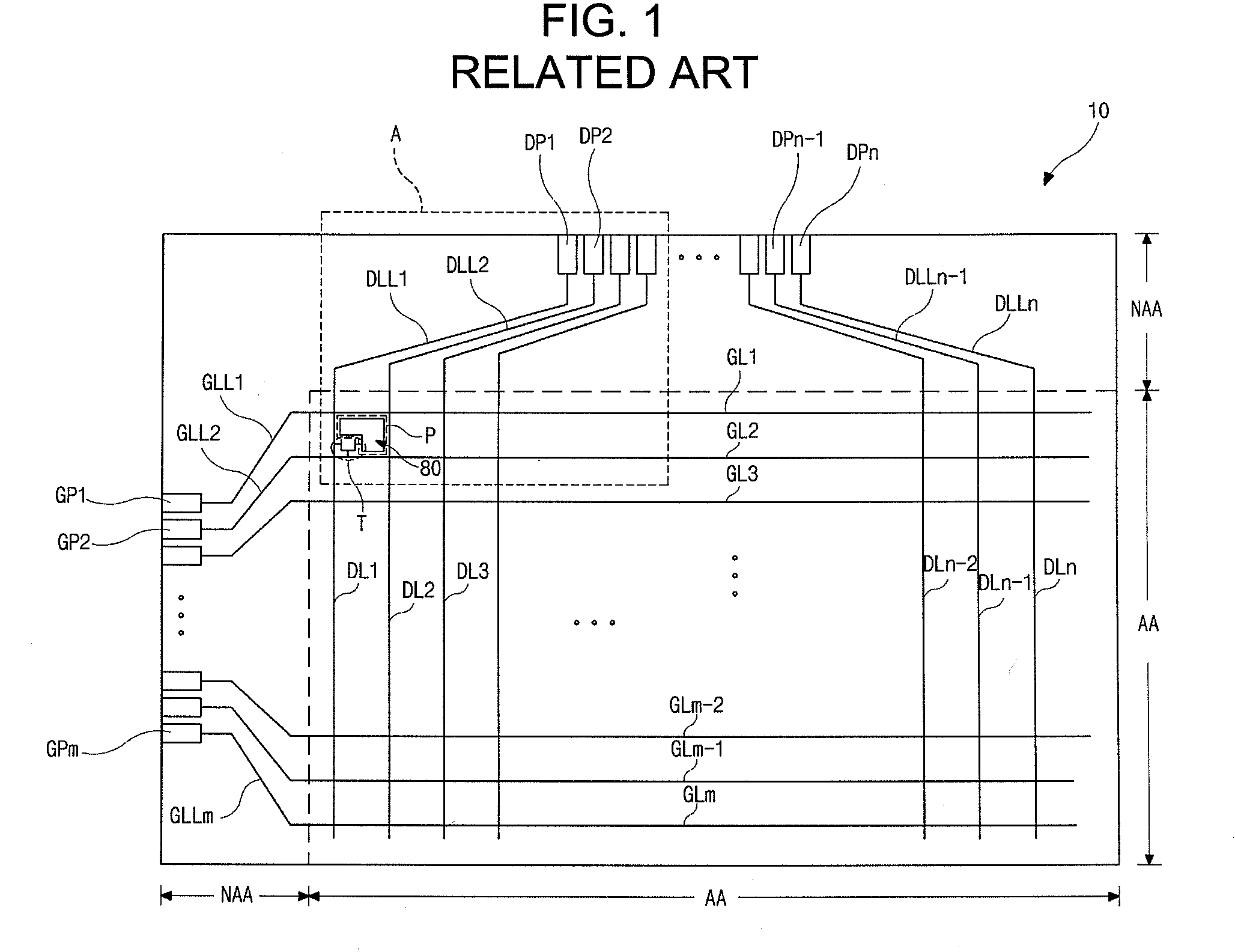
[0038]Referring to FIG. 3, the array substrate includes a display region AA to display images and a non-display region NAA.

[0039]In the display region AA, the array substrate includes first to mth gate lines GL1 to GLm each extended in a first direction and first to nth data lines DL1 to DLn each extended in a second direction and crossing the first to mth gate lines GL1 to GLm to define a plurality of pixel regions P in a matrix form.

[0040]A thin film transistor T is located in each pixel region P and connected to the corresponding gate and data lines. A pixel electrode 180 is located in each pixel region P and connected to the thin film transistor T. The pixel electrode 180 may be formed of a transparent conductive material including indium-tin-oxide (ITO), indium-zinc-oxide (IZO) and indium-tin-zinc-oxide (ITZO). When the LCD device is an in-plane switching mode LCD dev...

third embodiment

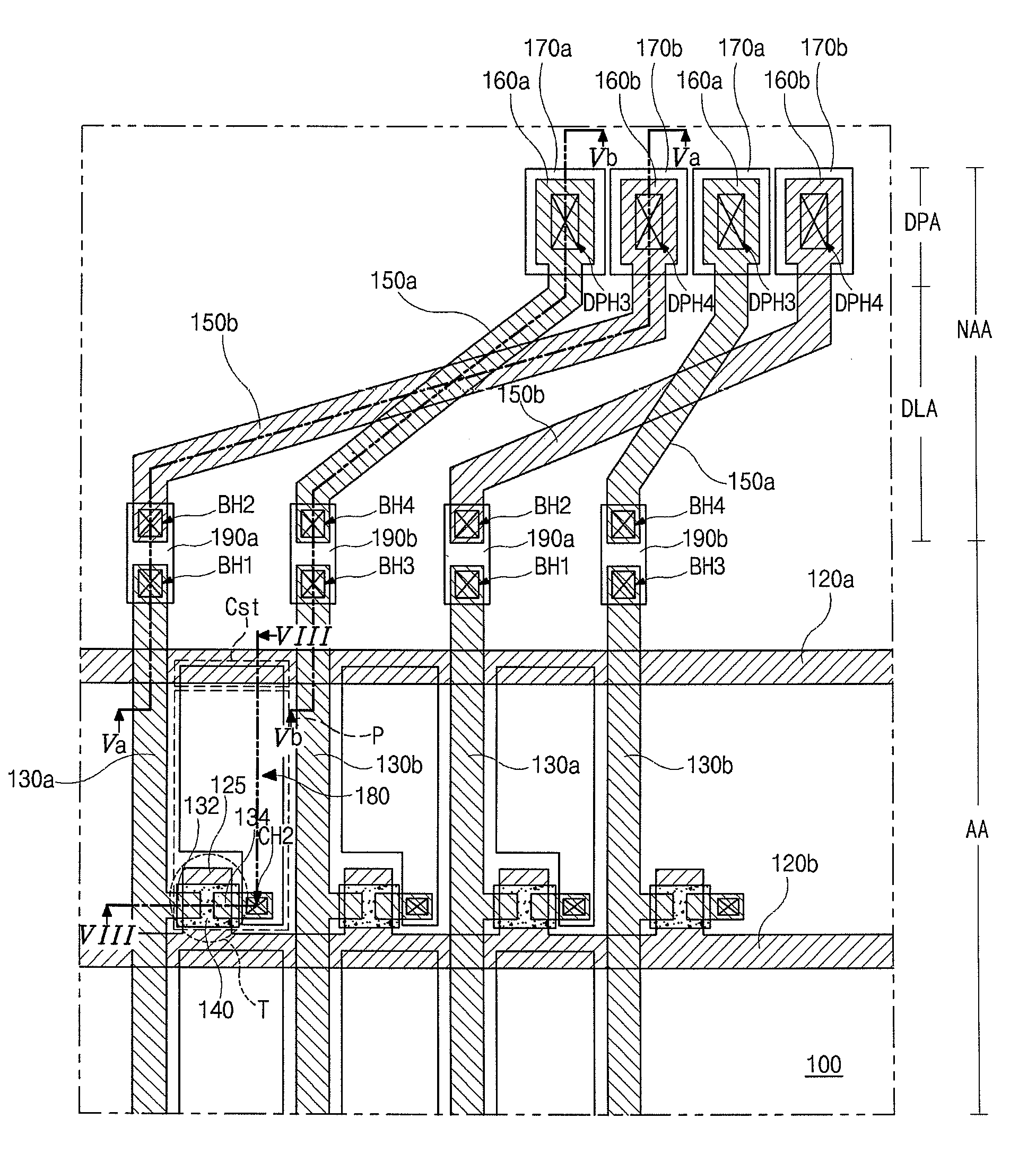
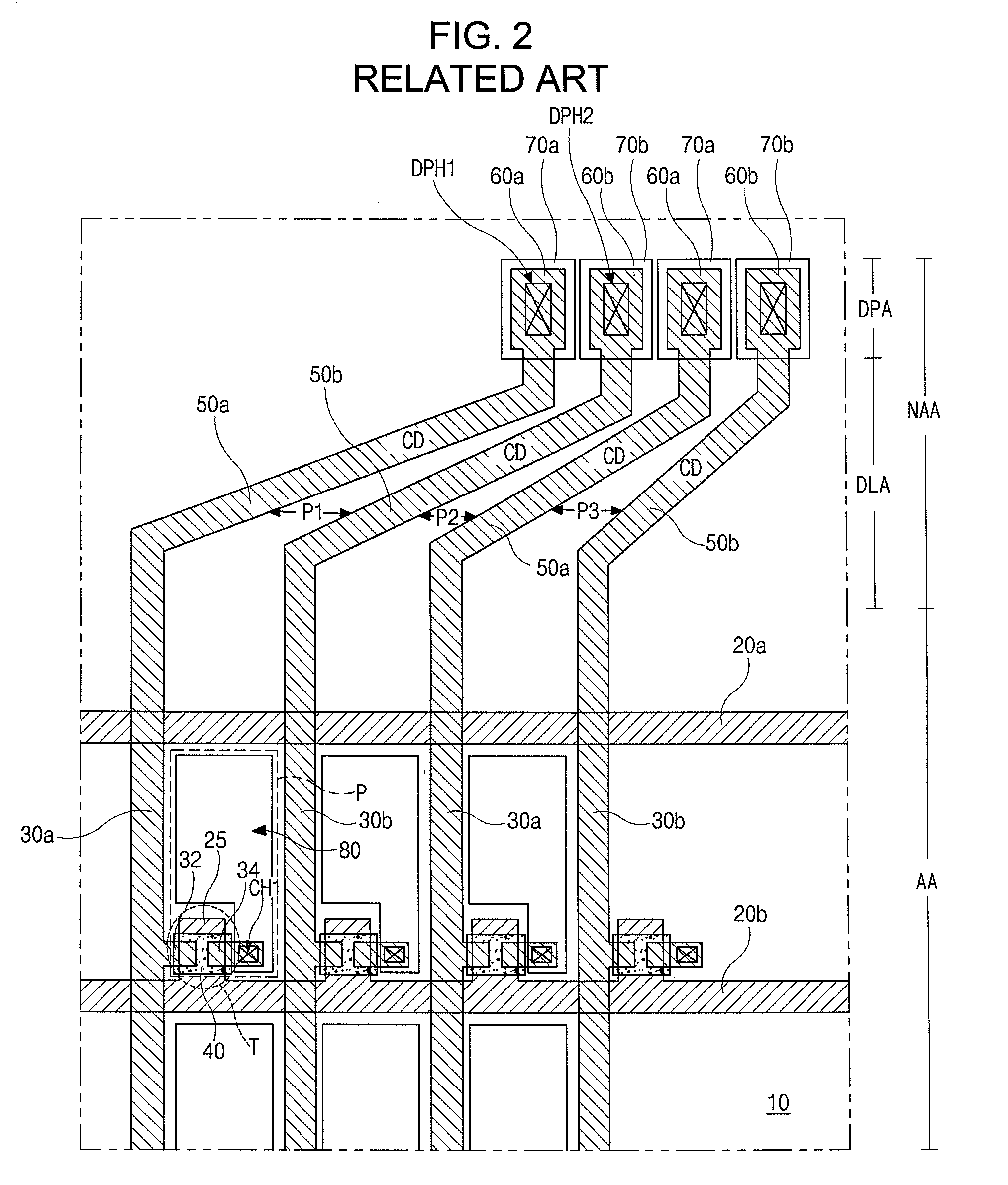
[0077]In the array substrate it is explained that the odd data link line 350a and the odd data pad electrode 360a are formed at the same layer as the gate line 320a and 320b, and the even data link line 350b and the even data pad electrode 360b are formed at the same layer as the data line 330a and 330b. Alternatively, the odd data link line 350a and the odd data pad electrode 360a may be formed at the same layer as the data line 330a and 330b, and the even data link line 350b and the even data pad electrode 360b are formed at the same layer as the gate line 320a and 320b.

[0078]As described in the embodiments of the present invention, since the odd and even data link lines are formed at different layers with the gate insulating layer therebetween, short-circuit between the even and odd data link lines can be prevented, and the data link region and the non-display region can be minimized. Further, since the bridge patterns are used, the resistance difference between the metal lines...


PUM

PropertyMeasurementUnit
electric fieldaaaaaaaaaa
areaaaaaaaaaaa
areasaaaaaaaaaa

Abstract

A liquid crystal display device includes a gate line on a substrate including a display region and a non-display region; odd and even data lines crossing the gate line to define a pixel region in the display region; a thin film transistor connected to the gate line and one of the odd and even data lines; a pixel electrode in the pixel region and connected to the thin film transistor; first and second data link lines electrically connected to the odd and even data lines, respectively, and formed with a gate insulating layer therebetween; and first and second data pad electrodes at one ends of the first and second data link lines, respectively.

Description

[0001]The present invention claims the benefit of Korean Patent Application No. 2007-0104092, filed in Korea on Oct. 16, 2007, which is hereby incorporated by reference for all purposes as if fully set forth herein.BACKGROUND OF THE INVENTION[0002]1. Field of the Invention[0003]The present invention relates to a liquid crystal display device, and more particularly, to a liquid crystal display (LCD) device and a method of manufacturing the same.[0004]2. Discussion of the Related Art[0005]Until recently, display devices have typically used cathode-ray tubes (CRTs). Presently, many efforts and studies are being made to develop various types of flat panel displays, such as liquid crystal display (LCD) devices, plasma display panels (PDPs), field emission displays, and electro-luminescence displays (ELDs), as a substitute for CRTs. Of these flat panel displays, LCD devices have many advantages, such as high resolution, light weight, thin profile, compact size, and low voltage power suppl...

Claims


Application Information

Patent Timeline
Patent Type & Authority Patents(United States)
IPC IPC(8): G02F1/1345G02F1/1333
CPCH01L27/1259G02F1/1345G02F1/1343G02F1/136
Inventor KWON, JANG-UNLEE, SU-WOONG
Owner LG DISPLAY CO LTD
Why Eureka
Try Eureka