Load driving device

a technology of driving device and load, which is applied in the direction of pulse technique, process and machine control, instruments, etc., can solve the problems of output transistor gate voltage not reaching a sufficiently high level, output transistor may be destroyed, and ground voltage supply to the load driving device may be interrupted

Active Publication Date: 2014-01-28
RENESAS ELECTRONICS CORP
View PDF29 Cites 2 Cited by
  • Summary
  • Abstract
  • Description
  • Claims
  • Application Information

AI Technical Summary

Benefits of technology

[0022]With the circuit configurations described above, an increase in consumption current can be suppressed in the standby state when the power supply is normally connected.
[0023]According to exemplary aspects of the present invention, it is possible to provide a load driving device capable of suppressing an increase in consumption current in the standby state when the power supply is normally connected.

Problems solved by technology

In this case, the supply of the ground voltage to the load driving device may be interrupted due to a defective connector, disconnection of a wire, or the like.
When the ground terminal is in the open state, there is a possibility that an output transistor having a function of switching between the load and the power supply becomes conductive, although a gate voltage of the output transistor has not reached a sufficiently high level.
This causes a problem that the output transistor may be destroyed due to overheating.
Specifically, a loss occurs in which, in the case where the load driving device of the prior art shown in FIG. 14 is integrated on a semiconductor substrate, when the load driving device is operated at a high voltage within operating conditions, vertical parasitic bipolar transistors Q4 to Q7 formed to the transistors MN4, MN6, and MN7 become conductive, thereby generating a consumption current.
This leads to an increase in the consumption current of the load driving device of the prior art.
This causes a problem that a current flows through the parasitic bipolar transistors and the consumption current increases in the load driving device.

Method used


Image

  • Load driving device
  • Load driving device
  • Load driving device

Examples


first exemplary embodiment

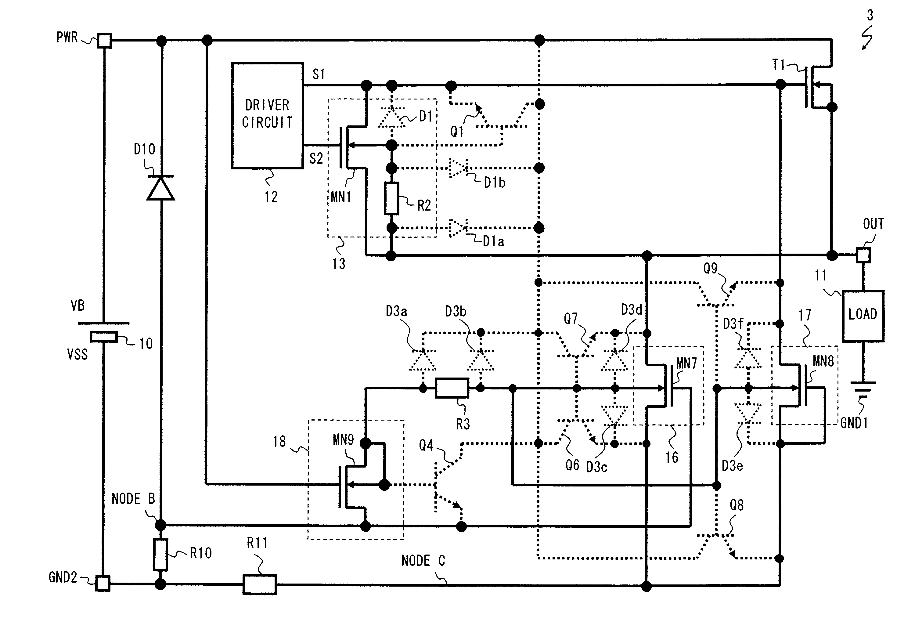
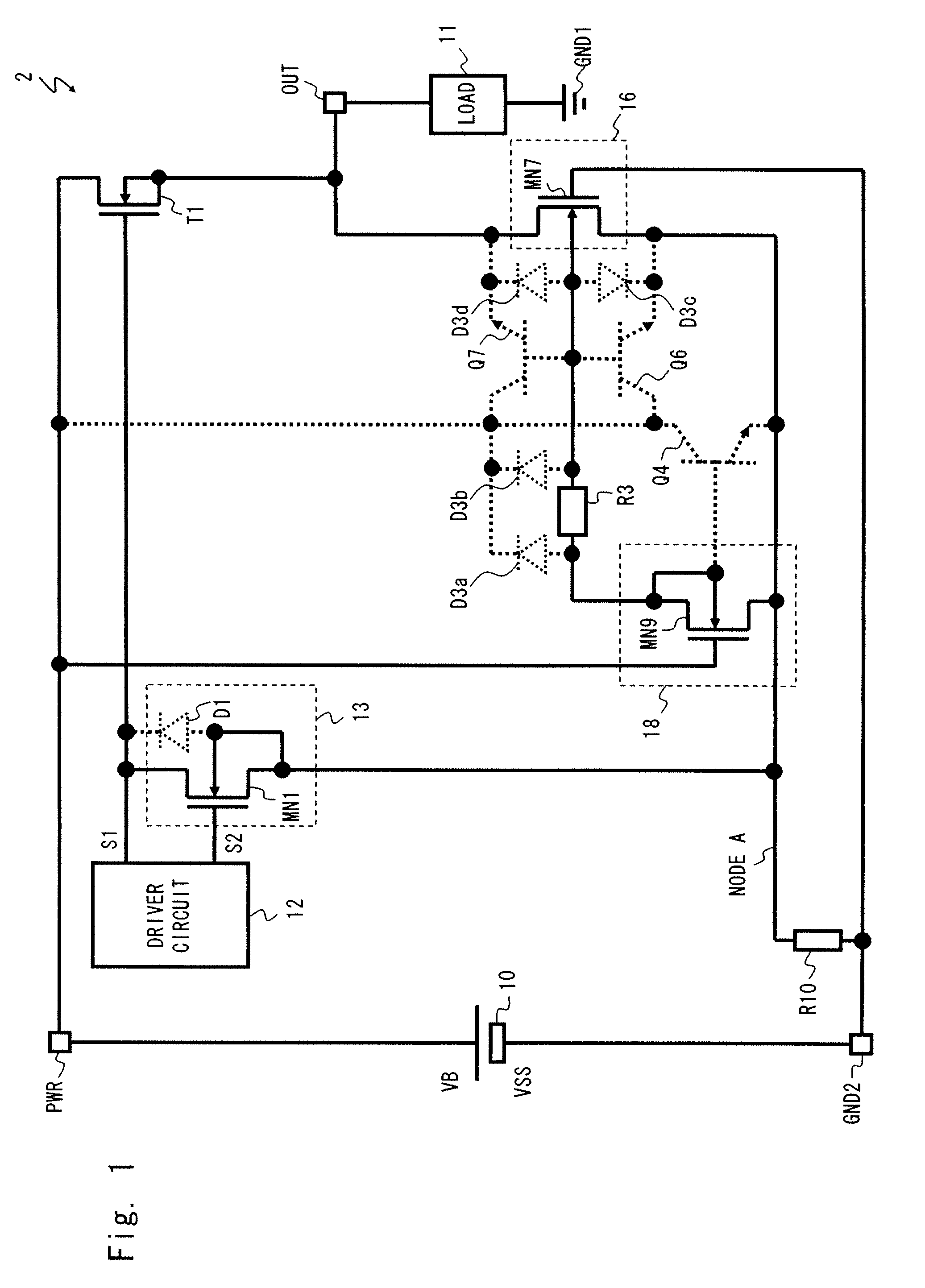
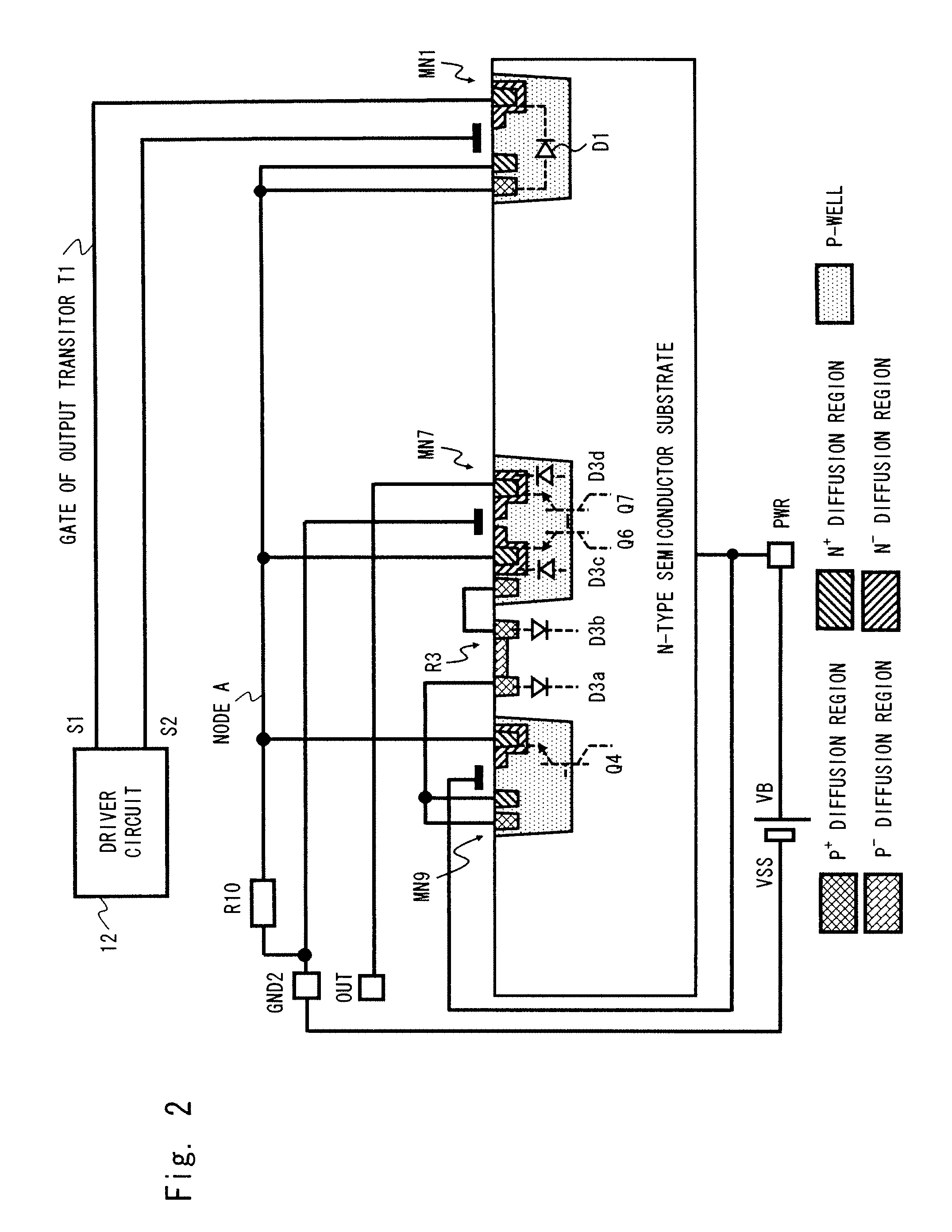
[0040]FIG. 1 shows a circuit diagram of a load driving device 2 according to a first exemplary embodiment of the present invention. As shown in FIG. 1, the load driving device 2 includes a power supply 10, a load 11, a driver circuit 12, a control circuit 13, a back gate control circuit 18, a compensation circuit 16, an output transistor T1, a resistor (a second resistor) R10, a resistor (a first resistor) R3, a power supply terminal PWR, a ground terminal GND1, a ground terminal GND2, and an output terminal OUT. The resistor R3 is a diffusion resistor, for example. In the first exemplary embodiment, a wiring line that couples the power supply 10 and the output transistor T1 through the power supply terminal PWR is referred to as a first power supply line; and a wiring line that couples the power supply 10 through the ground terminal GND2 is referred to as a second power supply line.

[0041]The power supply 10 is coupled between the power supply terminal PWR and the ground terminals G...

second exemplary embodiment

[0070]The load driving device 2 described above can prevent a malfunction associated with the off state of the output transistor T1 due to an increase in voltage of the ground terminal GND2. However, it is difficult to protect the load driving device 2 in the case where the power supply 10 is reversely connected. Meanwhile, according to a second exemplary embodiment of the present invention, it is possible to achieve the prevention of a malfunction associated with the off state of the output transistor T1 due to an increase in voltage of the ground terminal GND2, as well as the protection of the load driving device when the power supply 10 is reversely connected.

[0071]Furthermore, the second exemplary embodiment can solve the following problem. That is, as described above, when the load driving device is used for a vehicle or the like, the ground terminal GND1 on the load 11 side and the ground terminal GND2 on the control circuit 13 side are grounded at different points. Accordingl...

third exemplary embodiment

[0100]FIG. 7 is a circuit diagram of a load driving device 4 according to a third exemplary embodiment of the present invention. FIG. 8 shows a sectional view illustrating devices constituting the load driving device 4 according to the third exemplary embodiment. FIG. 9 shows a circuit diagram of the load driving device 4 when the power supply is reversely connected, and FIG. 10 shows a sectional view illustrating devices constituting the load driving device 4 when the power supply is reversely connected. The load driving device 4 includes a back gate control circuit 18b as a modified example of the back gate control circuit 18 of the load driving device 3. Components of the load driving device 4 similar to those of the load driving device 3 are denoted by the same reference symbols, and the description thereof is omitted.

[0101]In comparison with the back gate control circuit 18 of the load driving device 3, the back gate control circuit 18b of the load driving device 4 causes the b...


PUM


Abstract

A load driving device according to an exemplary aspect of the present invention includes: an output transistor coupled between a first power supply line and an output terminal; the output terminal being configured to be coupled with a load; a driver circuit that controls conduction / non-conduction of the output transistor; a compensation transistor that is coupled between the output terminal and a second power supply line, and becomes conductive when the driver circuit renders the output transistor non-conductive and when a potential of the second power supply line reaches a predetermined value or greater, to maintain a non-conduction state of the output transistor; and a first resistor coupled between the second power supply line and a back gate of the compensation transistor.

Description

INCORPORATION BY REFERENCE[0001]This application is based upon and claims the benefit of priority from Japanese patent application No. 2009-254360, filed on Nov. 5, 2009, the disclosure of which is incorporated herein in its entirety by reference.BACKGROUND[0002]1. Field of the Invention[0003]The present invention relates to a load driving device, and more particularly, to a load driving device including an output transistor that controls power supply to a load.[0004]2. Description of Related Art[0005]Semiconductors for power supply have been widely employed as load driving devices that supply power from a power supply to a load. In one field of application, the semiconductors are used to drive actuators or lamps of vehicles.[0006]In such a load driving device, a ground terminal of the load driving device and a ground terminal of the load may be arranged apart from each other. In this case, a voltage difference may be generated between a ground voltage of the load driving device and...

Claims


Application Information

Patent Timeline
Patent Type & Authority Patents(United States)
IPC IPC(8): H02H9/04H02H3/20B25B7/22H02H3/00
CPCH03K2217/0018H03K17/0822H03K2217/0036H03K2017/066H03K17/063Y10T307/839
Inventor NAKAHARA, AKIHIRO
Owner RENESAS ELECTRONICS CORP
Why Eureka
Try Eureka