Integrated circuit with electrostatically coupled MOS transistors and method for producing such an integrated circuit

a technology of electrostatic coupling and integrated circuit, which is applied in the direction of transistors, electrical devices, semiconductor devices, etc., can solve the problems of difficult to obtain and difficulty in polarizing channels, and achieve high performance

Active Publication Date: 2014-10-07
COMMISSARIAT A LENERGIE ATOMIQUE ET AUX ENERGIES ALTERNATIVES
View PDF12 Cites 130 Cited by
  • Summary
  • Abstract
  • Description
  • Claims
  • Application Information

AI Technical Summary

Problems solved by technology

However, in the case where these elements are no longer correctly aligned in relation to each other, difficulties may then appear to polarize the channel 13b via the gate 17a.
It is, however, difficult to obtain, with this technique, a good alignment between the transistors of the different levels, the best results obtained making it possible to obtain an alignment in the vicinity of 100 nm.

Method used


Image

  • Integrated circuit with electrostatically coupled MOS transistors and method for producing such an integrated circuit
  • Integrated circuit with electrostatically coupled MOS transistors and method for producing such an integrated circuit
  • Integrated circuit with electrostatically coupled MOS transistors and method for producing such an integrated circuit

Examples


Embodiment Construction

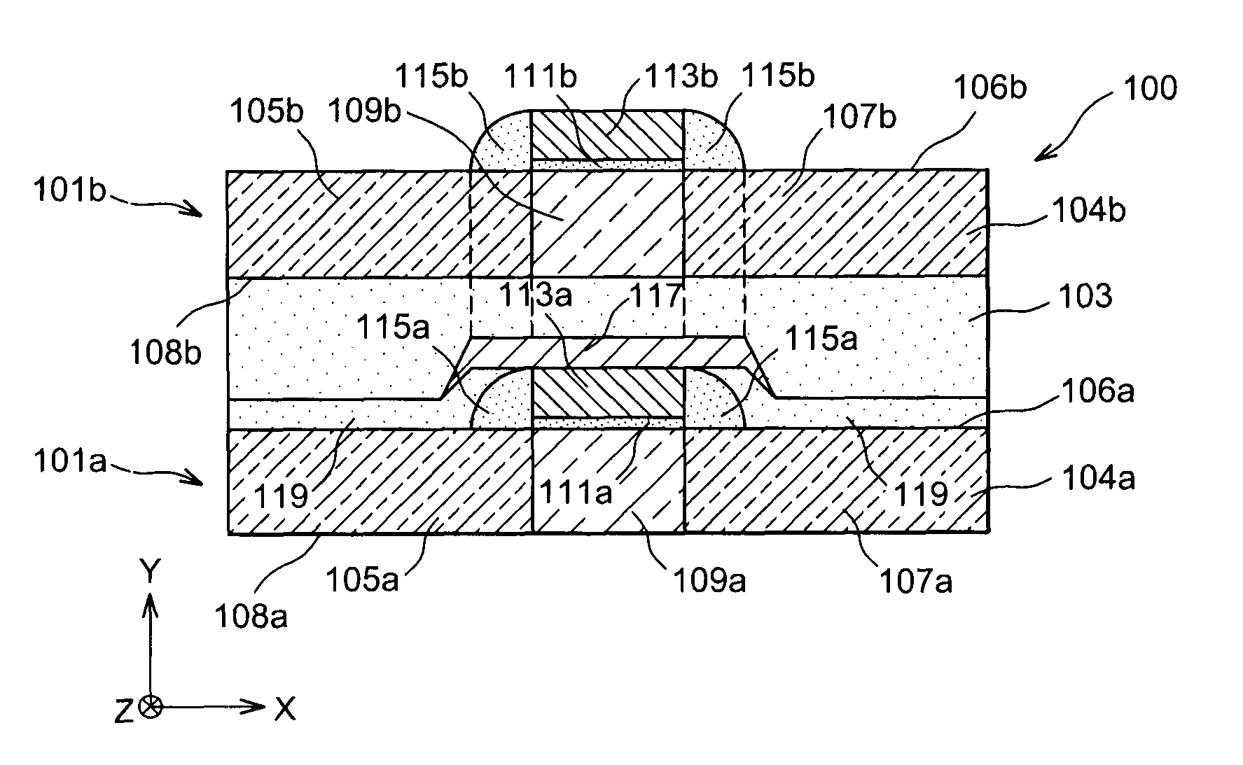
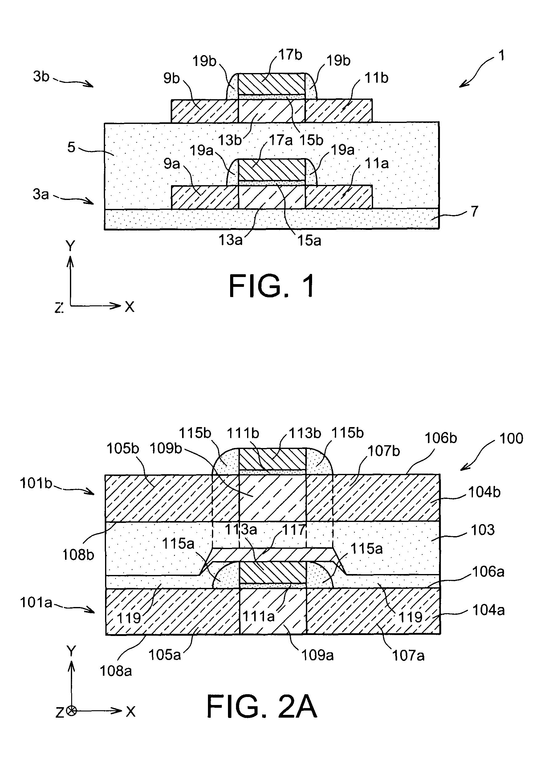
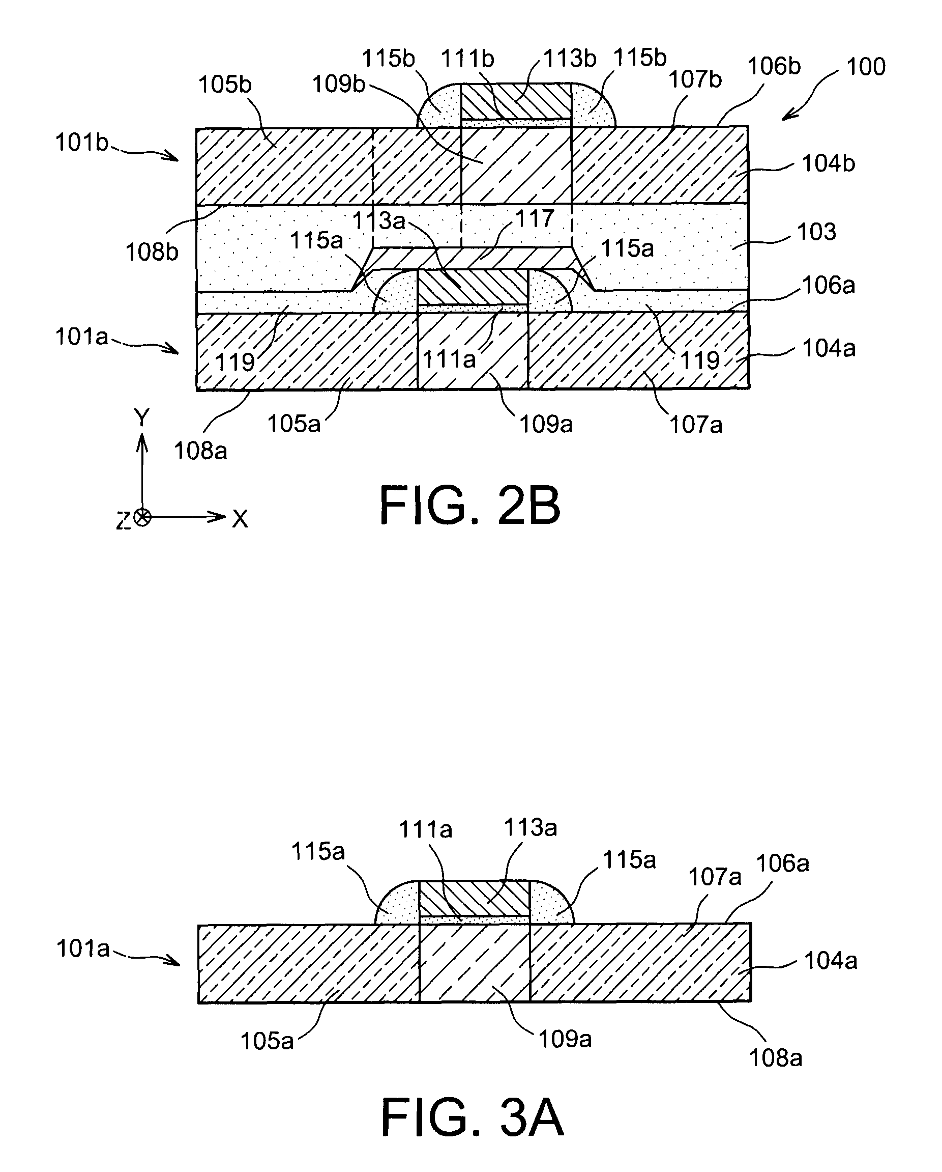
[0060]We will first refer to FIG. 2A, which illustrates one embodiment of an integrated circuit 100 with MOS transistors coupled to each other electrostatically, according to one specific embodiment.

[0061]In this FIG. 2A, the integrated circuit 100 includes two levels of MOS transistors. Furthermore, only two transistors 101a and 101b of the integrated circuit 100, superimposed one on top of the other, are shown in FIG. 2A. The upper transistor 101b is produced on a dielectric layer 103, for example SiO2-based, covering the lower transistor 101a, which is itself produced on a dielectric layer, not shown in FIG. 2A, which is for example the buried dielectric layer, for example SiO2-based, of a SOI (silicon on insulator) substrate. Alternatively, it is possible for the lower transistor 101a to be produced on a massive substrate, for example silicon. Each transistor 101a, 101b includes a portion of a layer, referenced 104a and 104b, respectively, composed of a semiconductor material, f...


PUM


Abstract

An integrated circuit including at least: a first MOS transistor; a second MOS transistor, arranged on the first MOS transistor, the second MOS transistor including a channel region in at least one semiconductor layer including two approximately parallel primary faces; a portion of at least one electrically conductive material electrically connected to a gate of the first transistor and arranged between the gate of the first transistor and the channel region of the second transistor; a dielectric layer arranged at least between the portion of the electrically conductive material and the channel region of the second transistor; and a section of the channel region of the second transistor in a plane parallel to the two primary faces of the semiconductor layer is included in a section of the portion of the electrically conductive material projected in said plane.

Description

TECHNICAL FIELD[0001]The invention concerns the field of integrated circuits with superimposed MOS transistors, i.e. which can include several stacked levels of MOS transistors, and coupled to each other electrostatically. The invention also concerns a method for producing such integrated circuits.BACKGROUND OF THE INVENTION[0002]In an integrated circuit including MOS transistors, these transistors are generally produced from a single semiconductor layer in which the channels of these transistors are formed. This semiconductor layer is topped with metal interconnections forming contacts electrically connected to the gates and to the source and drain regions of the transistors.[0003]In order to improve the integration density of the MOS transistors in the integrated circuits, it is known to produce integrated circuits including several stacked layers of transistors. One example of such an integrated circuit 1 is illustrated in FIG. 1. In this FIG. 1, only two transistors 3a and 3b, s...

Claims


Application Information

Patent Timeline
Patent Type & Authority Patents(United States)
IPC IPC(8): H01L27/088
CPCH01L27/1104H01L21/8221H01L27/0688H01L27/11H10B10/00H10B10/12
Inventor AUGENDRE, EMMANUELVINET, MAUDCLAVELIER, LAURENTBATUDE, PERRINE
Owner COMMISSARIAT A LENERGIE ATOMIQUE ET AUX ENERGIES ALTERNATIVES
Why Eureka
Try Eureka