Liquid crystal display device comprising a P-type liquid crystal material and a first alignment layer having an anchoring energy

a liquid crystal display and alignment layer technology, applied in non-linear optics, instruments, optics, etc., can solve problems such as light leakage (emission of irregularly polarized light), and achieve the effect of suppressing display defects due to collapse of liquid crystal alignmen

Active Publication Date: 2015-01-13
SHARP KK
View PDF56 Cites 0 Cited by
  • Summary
  • Abstract
  • Description
  • Claims
  • Application Information

AI Technical Summary

Benefits of technology

[0023]The present invention is devised in view of the above-described existing circumstances, and an object of the present invention is to provide a liquid crystal display device that can suppress a display defect due to collapse of liquid crystal alignment.
[0024]The present inventors have conducted studies on a liquid crystal display device that can suppress a display defect due to collapse of liquid crystal alignment, and they have paid attention to deformation of the liquid crystal, i.e., easiness of change in the liquid crystal alignment. Further, they have revealed that the deformation of the liquid crystal can be facilitated by reducing binding force of the liquid crystal on an alignment layer interface to make it easy to deform the liquid crystal, preparing a liquid crystal material that is easily deformed, and / or controlling a substrate interface to urge the deformation of the liquid crystal. More specifically, the deformation can be facilitated by (1) a conformation that the liquid crystal material has a bending elastic constant k33 of k33≦14 pN; (2) a conformation that the alignment layer has an anchoring energy of not greater than 1.5×10⁻⁴ J / m2; (3) a conformation that the alignment layer includes an alignment film having a fluorine-containing group; (4) a conformation that the alignment layer includes a chemisorption film; (5) a conformation that the alignment layer includes irregularities configured to control alignment of a p-type liquid crystal material; (6) a conformation that the p-type liquid crystal material contains liquid crystal molecules that previously tilt when no voltage is applied in a direction along which they tilt when a voltage is applied; and (7) a conformation that a comb-shaped electrode has a tilted portion on its surface on the liquid crystal layer side, or by a combination of these conformations. The present inventors have conceived of excellently solving the above-described problems, thereby attaining the present invention.
[0046]Introduction of a fluorine-containing group (a F-based functional group) causes reduction in the surface energy, thereby enabling smooth rotation of the liquid crystal molecules. Further, since the effect of this fluorine-containing group is enhanced as a ratio of fluorine atoms increases, introduction of a CF2 group is very effective.
[0052]According to the liquid crystal display device of the present invention, a display defect due to collapse of liquid crystal alignment can be suppressed.

Problems solved by technology

When an excessive voltage is applied, the liquid crystal alignment collapses in an inter-electrode region, and light leakage (emission of irregularly polarized light) occurs.

Method used


Image

  • Liquid crystal display device comprising a P-type liquid crystal material and a first alignment layer having an anchoring energy
  • Liquid crystal display device comprising a P-type liquid crystal material and a first alignment layer having an anchoring energy
  • Liquid crystal display device comprising a P-type liquid crystal material and a first alignment layer having an anchoring energy

Examples


embodiment 1

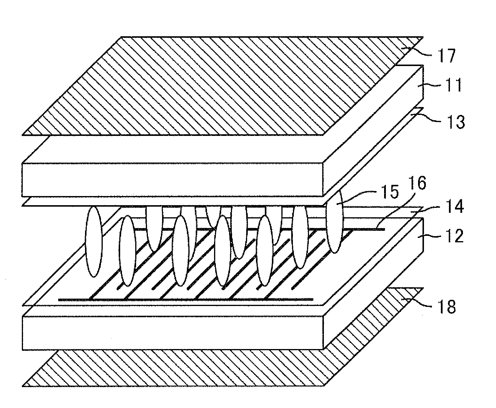
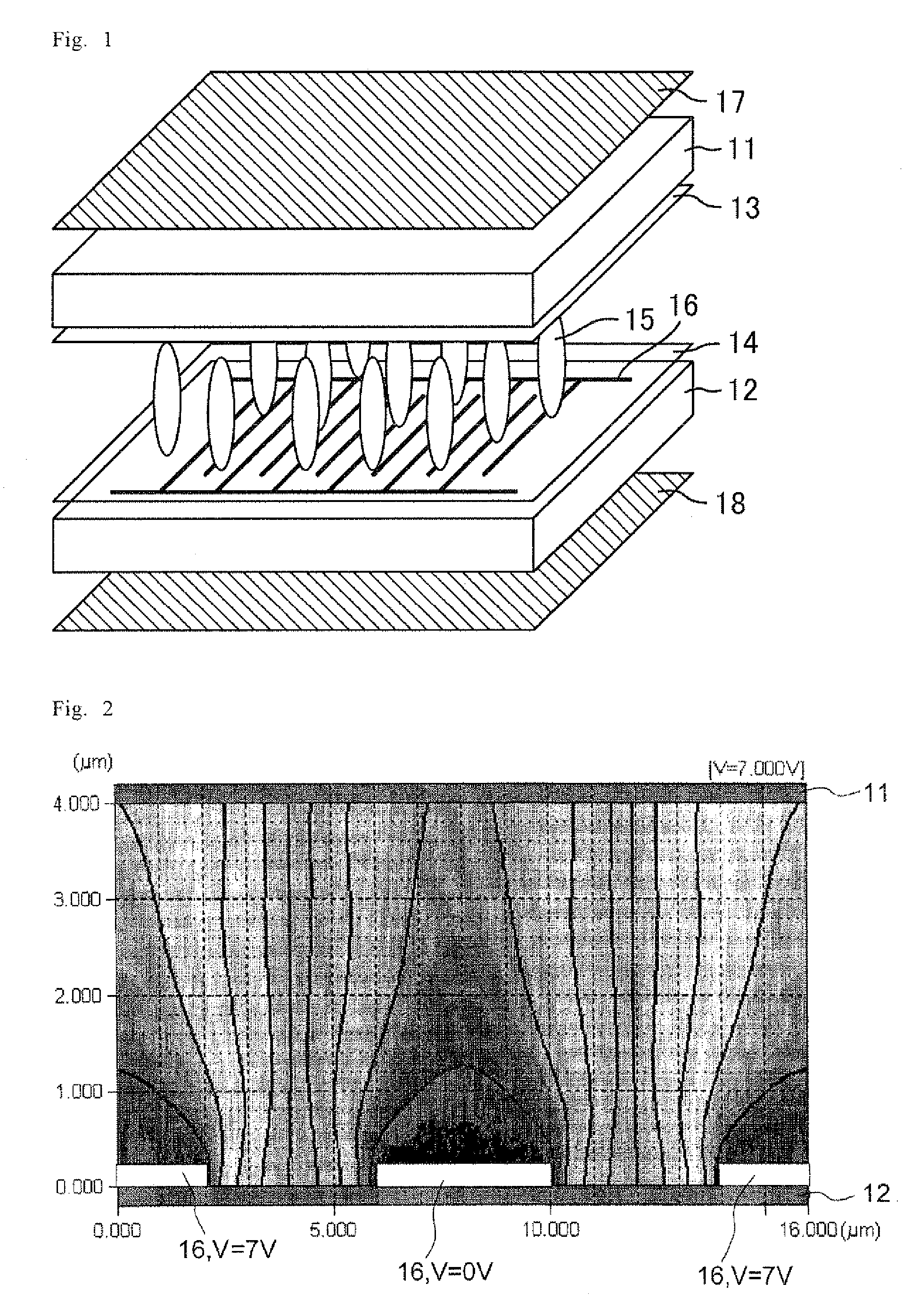
[0071]In a liquid crystal display device of the present embodiment, distribution of an electric field intensity is formed in a cell by applying an electric field, thereby achieving bend alignment of liquid crystal. Additionally, the liquid crystal display device of the present embodiment is a liquid crystal display device in which an electric field is applied to a homeotropically aligned p-type nematic liquid crystal (nematic liquid crystal having positive dielectric anisotropy) transversely with respect to a substrate surface, wherein a bending array is formed by the electric field application. Further, an alignment orientation of liquid crystal molecules is determined by the electric field. The electric field may have a component parallel to the substrate surface.

[0072]Further, the liquid crystal display device of the present embodiment includes a liquid crystal display element (cell), a driver circuit, and a backlight (an illumination device). Configurations of the driver circuit...

example 1

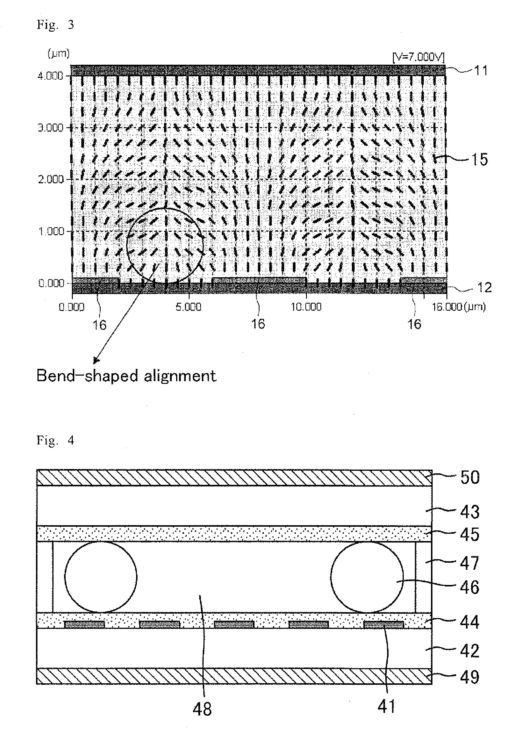
[0138]FIG. 4 shows a basic configuration of a liquid crystal display element used in a liquid crystal display device of Example 1. First, a polyimide homeotropic alignment film JALS-204 (JSR Corp., 5 wt. %, a γ-butyrolactone solution) was applied to a glass substrate (a lower substrate) 42 that has a comb-shaped electrode 41 comprising ITO by spin-coating. Then, the workpiece was baked at 200° C. for two hours. The film thickness of an alignment film (an alignment layer) 44 was 60 nm in this case.

[0139]In not only Example 1 but also all the examples, the electrode width was set to 4 μm, the electrode spacing was set to 4 μm, and the cell gap was set to 4 μm. Alignment disorder of the liquid crystal depends on electric field intensity. Since the effects of the present invention can be well understood by experiments with a narrower spacing, the electrode spacing (4 μm) that is relatively narrow among normally used electrode spacings was used in all the examples.

[0140]Likewise, an alig...

example 2

[0147]A basic configuration of a liquid crystal display element used in a liquid crystal display device of Example 2 is the same as that shown in FIG. 4. A liquid crystal cell having an electrode width of 4 μm, an electrode spacing of 4 μm, and a cell gap of 4 μm was fabricated by the following method.

[0148]First, a glass substrate 42 that has a comb-shaped electrode 41 comprising ITO was immersed in a 0.01-mol / l chloroform-NMP mixed solution (a mixing ratio (a volume ratio) of chloroform:NMP=1:10) containing a silane coupling material of formula (1) for five minutes. Then, this substrate was dried in dry nitrogen at 120° C. for one hour to form an alignment film (an alignment layer) 44 comprising a chemisorption film.

CF3CF2)17—SiCl3  (1)

[0149]Likewise, an alignment film (an alignment layer) 45 that consists of a chemisorption film comprising the same material as that of the alignment film 44 was formed on a glass substrate 43. Subsequently, 4-micron resin beads 46 (micro pearls SP,...


PUM

PropertyMeasurementUnit
pre-tilt angleaaaaaaaaaa

Abstract

The present invention provides a liquid crystal display device that can suppress a display defect due to collapse of liquid crystal alignment. The present invention provides a liquid crystal display device comprising a liquid crystal display element including a pair of substrates and a liquid crystal layer hermetically interposed between the pair of substrates, wherein the liquid crystal layer includes a p-type liquid crystal material that is homeotropically aligned with respect to surfaces of the pair of substrates when no voltage is applied; one of the pair of substrates comprises a comb-shaped electrode and a first alignment layer configured to control alignment of the p-type liquid crystal material; the other of the pair of substrates comprises a second alignment layer configured to control alignment of the p-type liquid crystal material; and the first alignment layer has an anchoring energy of not greater than 1.5×10⁻⁴ J / m2.

Description

[0001]This application is the U.S. national phase of International Application No. PCT / JP2010 / 054561 filed 17 Mar. 2010 which designated the U.S. and claims priority to JP Patent Application No. 2009-127932 filed 27 May 2009 and JP Patent Application No. 2010-006689 filed 15 Jan. 2010, the entire contents of each of which are hereby incorporated by reference.TECHNICAL FIELD[0002]The present invention relates to a liquid crystal display device. Specifically, the present invention relates to a liquid crystal display device suitable for a display mode of controlling light transmission by bend-deforming a liquid crystal layer by voltage application.BACKGROUND ART[0003]A liquid crystal display device is characterized in a low profile, a light weight, and low power consumption, and it is extensively used in various fields. Further, its display performance has greatly advanced with the lapse of time and has gained an advantage over a CRT (Cathode Ray Tube).[0004]A display mode of the liqui...

Claims


Application Information

Patent Timeline
Patent Type & Authority Patents(United States)
IPC IPC(8): G02F1/1337G02F1/1343G02F1/139
CPCG02F1/134363G02F1/1395G02F2001/133742G02F2001/134381G02F1/133742G02F1/134381
Inventor ISHIHARA, SHOICHISAKURAI, TAKEHISAMURATA, MITSUHIROKOZAKI, SHUICHIOHTAKE, TADASHI
Owner SHARP KK
Why Eureka
Try Eureka