Liquid crystal display device

a display device and liquid crystal technology, applied in static indicating devices, instruments, non-linear optics, etc., can solve problems such as limited area where signal lines are arranged, display defects such as flickering, and change in the potentials of pixel electrodes

Active Publication Date: 2019-08-15
SHARP KK
View PDF2 Cites 0 Cited by
  • Summary
  • Abstract
  • Description
  • Claims
  • Application Information

AI Technical Summary

Problems solved by technology

As a result, the difference of the timing when the gate signal shifts from ON to OFF causes a difference in the feedthrough voltage, leading to changes in the potentials of the pixel electrodes, and causing display defects such as flicker to occur.
Since driving circuits for driving the scanning lines are also provided in frame areas of the peripheral portions of the display area, the area where the signal lines are arranged is limited.
As the area for arranging the signal lines is smaller, the signal lines have to be arranged at narrower intervals, which makes it likely that signal lines would be short-circuited.

Method used


Image

  • Liquid crystal display device
  • Liquid crystal display device
  • Liquid crystal display device

Examples


embodiment 1

[0053]The following describes embodiments of the present invention in detail, while referring to the drawings. Identical or equivalent parts in the drawings are denoted by the same reference numerals, and the descriptions of the same are not repeated. To make the description easy to understand, in the drawings referred to hereinafter, the configurations are simply illustrated or schematically illustrated, or the illustration of part of constituent members is omitted. Further, the dimension ratios of the constituent members illustrated in the drawings do not necessarily indicate the real dimension ratios.

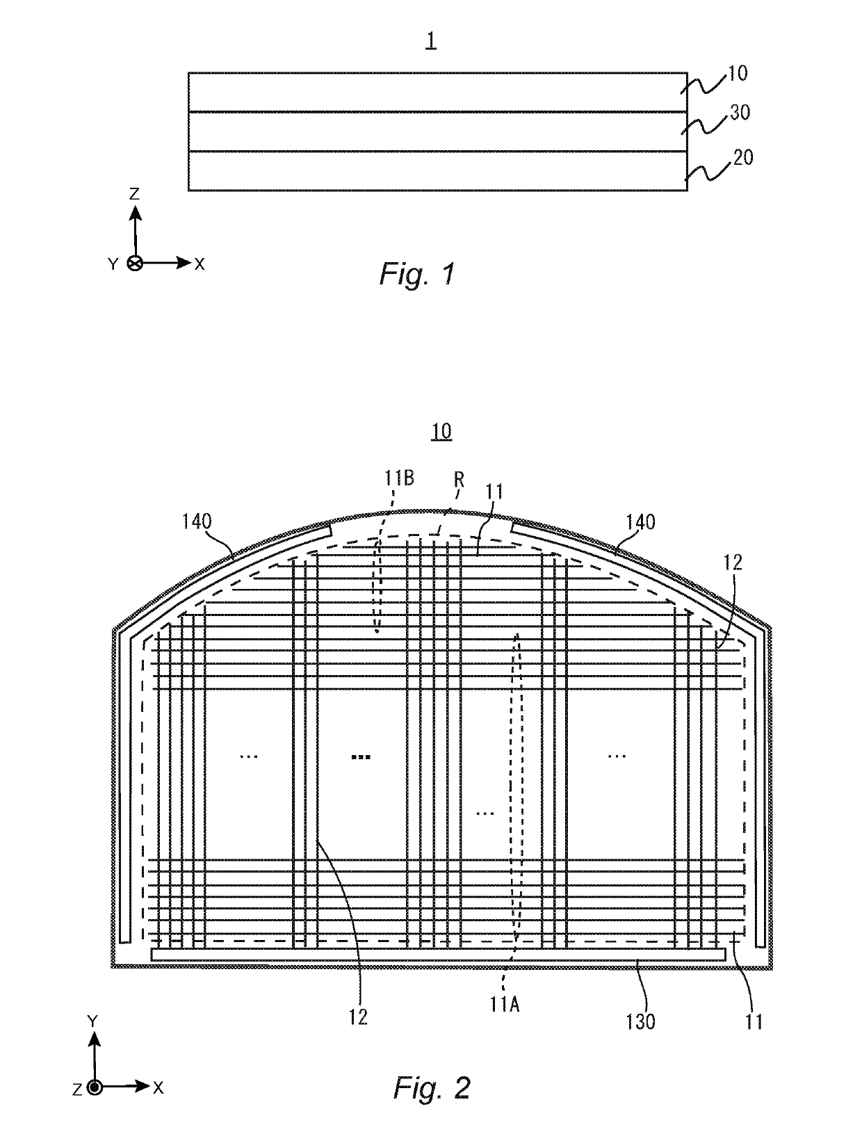
[0054]FIG. 1 is a cross-sectional view of a liquid crystal display device 1 in the present embodiment. The liquid crystal display device 1 in the present embodiment includes an active matrix substrate 10, a counter substrate 20, and a liquid crystal layer 30 interposed between the active matrix substrate 10 and the counter substrate 20. Further, though the illustration is omitted in ...

embodiment 2

[0091]The following description describes, as the present embodiment, a structure of the capacitance-generating part different from that of Embodiment 1. FIGS. 8 and 9 are cross-sectional views illustrating an exemplary capacitance-generating part in the present embodiment. In FIGS. 8 and 9, members identical to those in Embodiment 1 are denoted by the same reference symbols as those in Embodiment 1. The following description describes the configuration of each capacitance-generating part illustrated in FIGS. 8 and 9, principally regarding points different from those in Embodiment 1.

[0092]A capacitance-generating part Ca illustrated in FIG. 8 is different from the capacitance-generating part in Embodiment 1 in the point that the metal film (source layer) 103 and the semiconductor layer 102 are not provided below the transparent electrode film 104. In other words, the upper electrode 151 of the capacitance-generating part C in Embodiment 1 is composed of the transparent electrode fil...

embodiment 3

[0100]Embodiments 1 and 2 are described above with reference to an exemplary configuration of the upper electrode in the capacitance-generating part in which only the transparent electrode film 104, or the transparent electrode film 104 and the metal film 103, are connected to the common electrode 15 provided in the capacitance-generating area RC. As the present embodiment, an exemplary configuration is described in which the common electrode 15 provided in the capacitance-generating area RC functions as an upper electrode, and a lower electrode has a configuration different from that in Embodiments 1 and 2.

[0101]FIG. 11 is a cross-sectional view illustrating a capacitance-generating part in the present embodiment. As illustrated in FIG. 11, a capacitance-generating part Cc in the present embodiment is not provided with the semiconductor layer 102, as is the case with Embodiment 2. In the capacitance-generating part Cc, a lower electrode 161 is composed of the electrode 16, a metal ...


PUM

PropertyMeasurementUnit
capacitanceaaaaaaaaaa
thicknessaaaaaaaaaa

Abstract

Provided is a technique of suppressing display defects such as flicker, without limiting the arrangement of data lines, in a liquid crystal display device having a display area in a non-rectangular shape. A liquid crystal display device includes an active matrix substrate 10, a counter substrate, and a liquid crystal layer. The active matrix substrate 10 includes a plurality of gate lines 11, and a plurality of data lines 12. In each of pixels defined by the gate lines 11 and the data lines 12, a pixel electrode 14 is arranged, and in a display area R, common electrodes 15 are provided. Outside the display area R, capacitance-generating parts C that generate capacitances between some gate lines 11 among the plurality of gate lines 11 and the common electrode are provided. The some gate lines 11 have lengths smaller than the gate lines having the maximum length, and intersect with some data lines 12 among the plurality of data lines 12. The capacitance-generating parts C are provided in such a manner that at least one capacitance-generating part C is provided with respect to one of the some gate lines 11.

Description

TECHNICAL FIELD[0001]The present invention relates to a liquid crystal display device.BACKGROUND ART[0002]In a liquid crystal display device, a thin film transistor (TFT) is provided at a position at which a gate line (scanning line) and a data line intersect in an active matrix substrate, and the TFT is connected with a pixel electrode. In such a liquid crystal display device, a voltage change in a drain voltage of the TFT, which is called a feedthrough voltage, occurs due to a parasitic capacitance formed between a gate electrode of the TFT and the drain electrode connected with a pixel electrode, when a gate signal shifts from ON to OFF. This causes the potential of the pixel electrode to decreases by the feedthrough voltage. For example, in a case where a display area has a non-rectangular shape such as a circular shape, the lengths of the gate lines are not uniform, the number of data lines intersecting with each gate line varies, and the number of the TFTs connected with each ...

Claims


Application Information

Patent Timeline
Patent Type & Authority Applications(United States)
IPC IPC(8): G02F1/1362G02F1/1343G02F1/1333G02F1/1368G02F1/1345G02F1/1335
CPCG02F1/13452G02F1/133512G02F1/1368G02F2201/56G02F1/1345G09G3/3648G09G2320/0219G09G2300/0426
Inventor HORIUCHI, SATOSHIGYOUTEN, SEIJIROUTSUJINO, SACHIOKAWAMURA, TAKEHIKOMORINAGA, JUNICHI
Owner SHARP KK
Why Eureka
Try Eureka