Organic light-emitting diode package structure and method for forming the same
a light-emitting diode and organic technology, applied in the field of display technology, can solve the problems of oled package structure problems, oled light-emitting layer and an electrode to fail, and affect the service life of the oled devi
- Summary
- Abstract
- Description
- Claims
- Application Information
AI Technical Summary
Benefits of technology
Problems solved by technology
Method used
Image
Examples
first embodiment
A First Embodiment
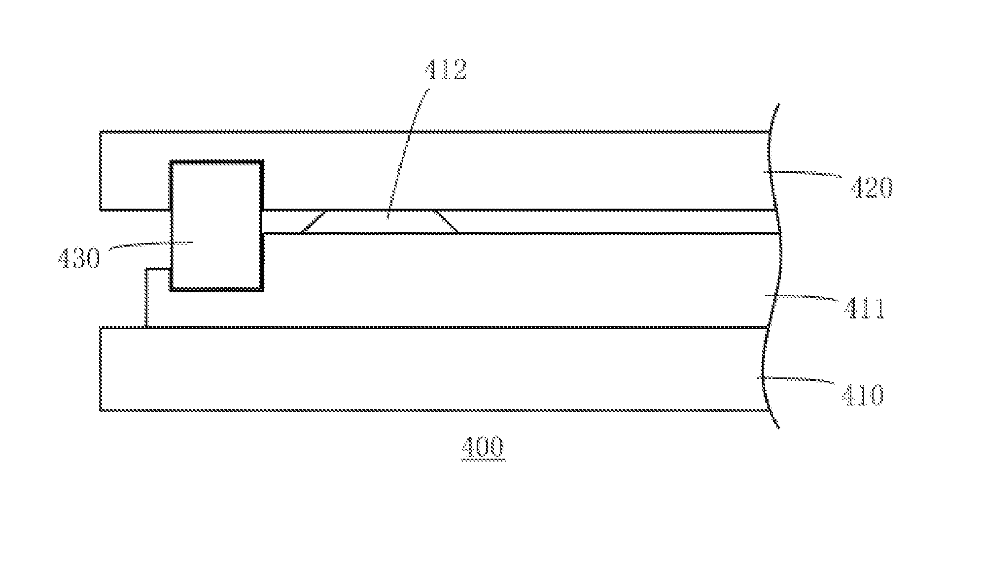
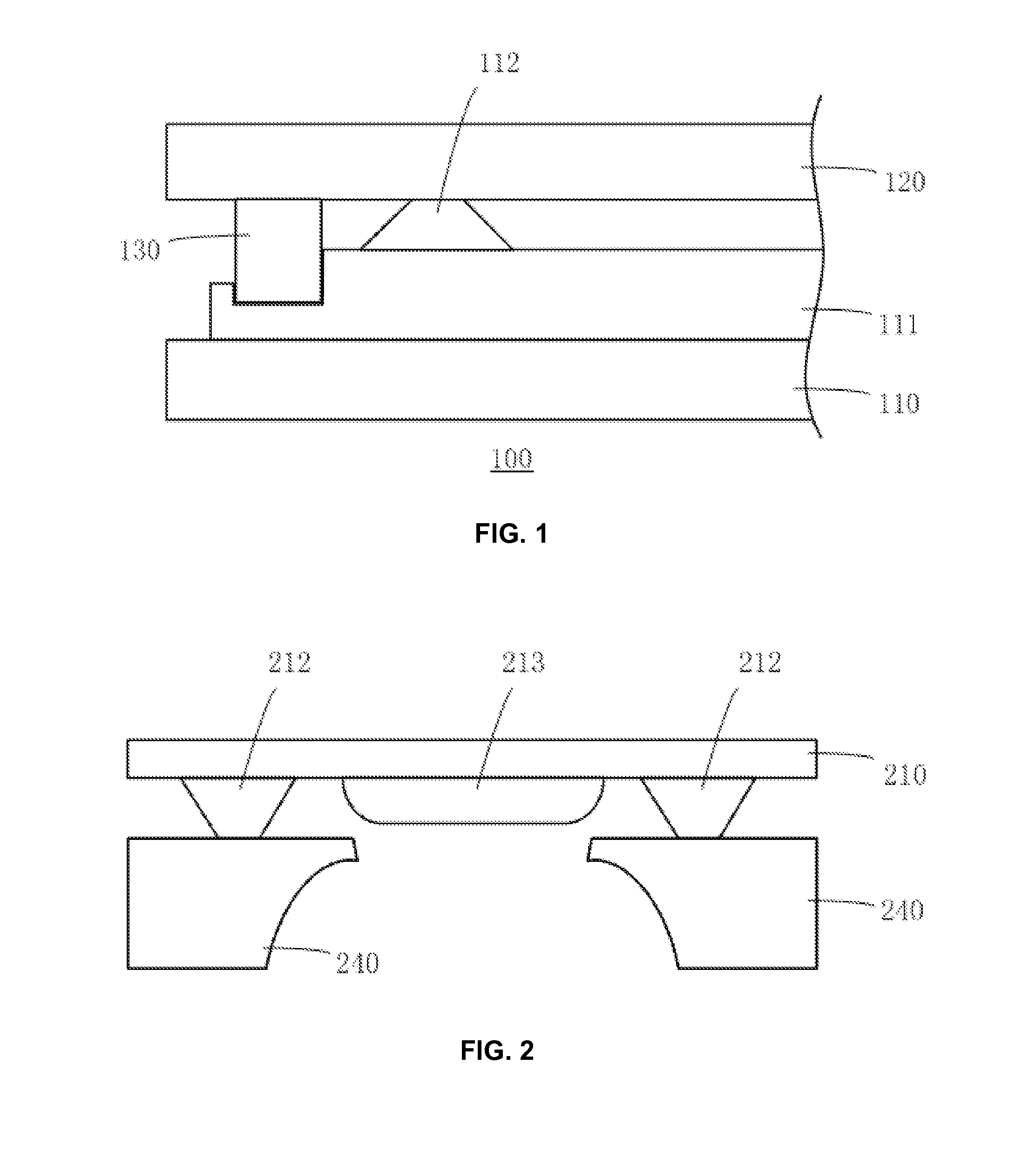
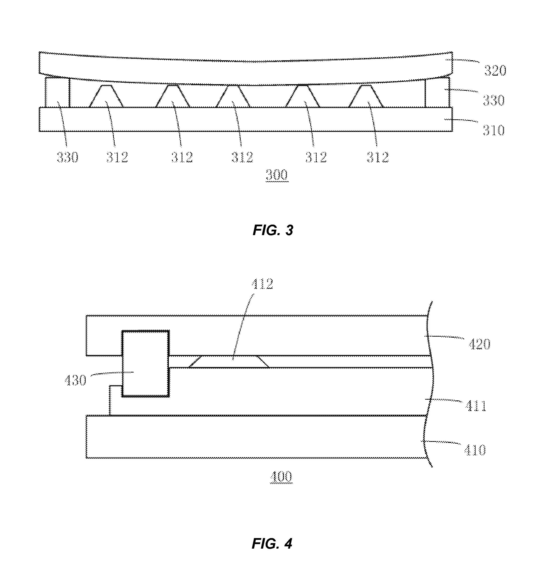
[0015]As shown in FIG. 4, an OLED package structure 400 according to an embodiment is shown. The OLED package structure 400 includes a substrate 410, a cover plate 420 and a packaging adhesive 430. On the substrate 410, an organic light-emitting element 411 including an OLED (not shown in the Figure) is provided. An annular groove is on the periphery of the inner surface of the cover plate 420 and surrounds the organic light-emitting element 411. As shown, the groove is located where the packaging adhesive 430 extends into the cover plate 420. The thickness of the packaging adhesive 430 is greater than the depth of the groove, so that a portion of the packaging adhesive 430 is in the groove of the cover plate 420, and a portion of the packaging adhesive 430 extends outside the groove of the cover plate 420. The cover plate 420 and the substrate 410 are adhered to each other by the packaging adhesive 430, so as to seal the organic light-emitting element 411.
[0016]It...
second embodiment
A Second Embodiment
[0023]A method for forming an OLED package structure, including Step S1 to Step S5 is described below. It should be noted that, in the method, the steps are named as S1 to S5 for distinguishing the steps conveniently and not for limiting the sequencing of the steps. In different embodiments according to the present invention, the sequencing of the steps may be adjusted. Steps S1 to S5 are described in conjunction with FIG. 4 to FIG. 7. The OLED package structure 400 as shown in FIG. 4 is formed with Steps S1 to S5 (corresponding to structures shown in FIG. 5 to FIG. 7) in the embodiment.
[0024]In Step S1, an entire substrate including multiple substrate units is provided. Each substrate unit includes an organic light-emitting element.
[0025]With reference to FIG. 5, the entire substrate 510 includes multiple substrate units. As shown in FIG. 5, in this embodiment, only a portion of one substrate unit of the entire substrate 510 is shown for convenience of illustrati...
PUM
 Abstract
Description
Claims
Application Information


