Organic light-emitting diode package structure and method for forming the same

Active Publication Date: 2014-06-26
SHANGHAI TIANMA MICRO ELECTRONICS CO LTD
View PDF2 Cites 10 Cited by
  • Summary
  • Abstract
  • Description
  • Claims
  • Application Information

AI Technical Summary

Benefits of technology

[0017]In some embodiments, multiple spacers 412 (only one is shown in FIG. 4) are provided between the organic light-emitting element 411 and the cover plate 420. In the OLED package structure 400 according to the embodiment shown, a portion of the packaging adhesive 430 is fixed in the groove of the cover plate 420. Therefore, the distance between the cover plate 420 and the substrate 410 adhered with the packaging adhesive 430 can be reduced with the packaging being not affected, and thus the thickness of the spacer 412 may be smaller. Since the thickness of the spacers 412 is smaller, evaporated materials at undesirable places may be reduced or eliminated. Accordingly, a color mixture phenomenon is prevented from occurring in the OLED package structure 400. Moreover, since the thickness of the spacers 412 is equal to the distance between the cover plate 420 and the substrate 410, in this case the spacers 412 may ensure a uniform distance between the cover plate 420 and the substrate 410, so that the Newton ring phenomenon is prevented form occurring in the entire OLED package structure 400.

Problems solved by technology

However, in an OLED device, it is possible for an organic light-emitting layer and an electrode to fail if they encounter with water or oxygen.
Accordingly, thereby service life of the OLED device is affected greatly.
In an early packaging method, since it has been impossible to ensure a good sealing, typically a desiccant or drier sheet has been provided inside the OLED device.
However, it has been unnecessary to use the desiccant or drier sheet inside the OLED device since frit sealing has been used as a packaging adhesive, as the frit is heated and melted by using a moving laser beam and can form a seal structure with good air-tightness.
However, there is a new problem for the OLED package structure using a frit as the packaging adhesive.
The unwanted evaporation material may cause poor display quality, such as poor color mixture of the display device.

Method used


Image

  • Organic light-emitting diode package structure and method for forming the same
  • Organic light-emitting diode package structure and method for forming the same
  • Organic light-emitting diode package structure and method for forming the same

Examples


first embodiment

A First Embodiment

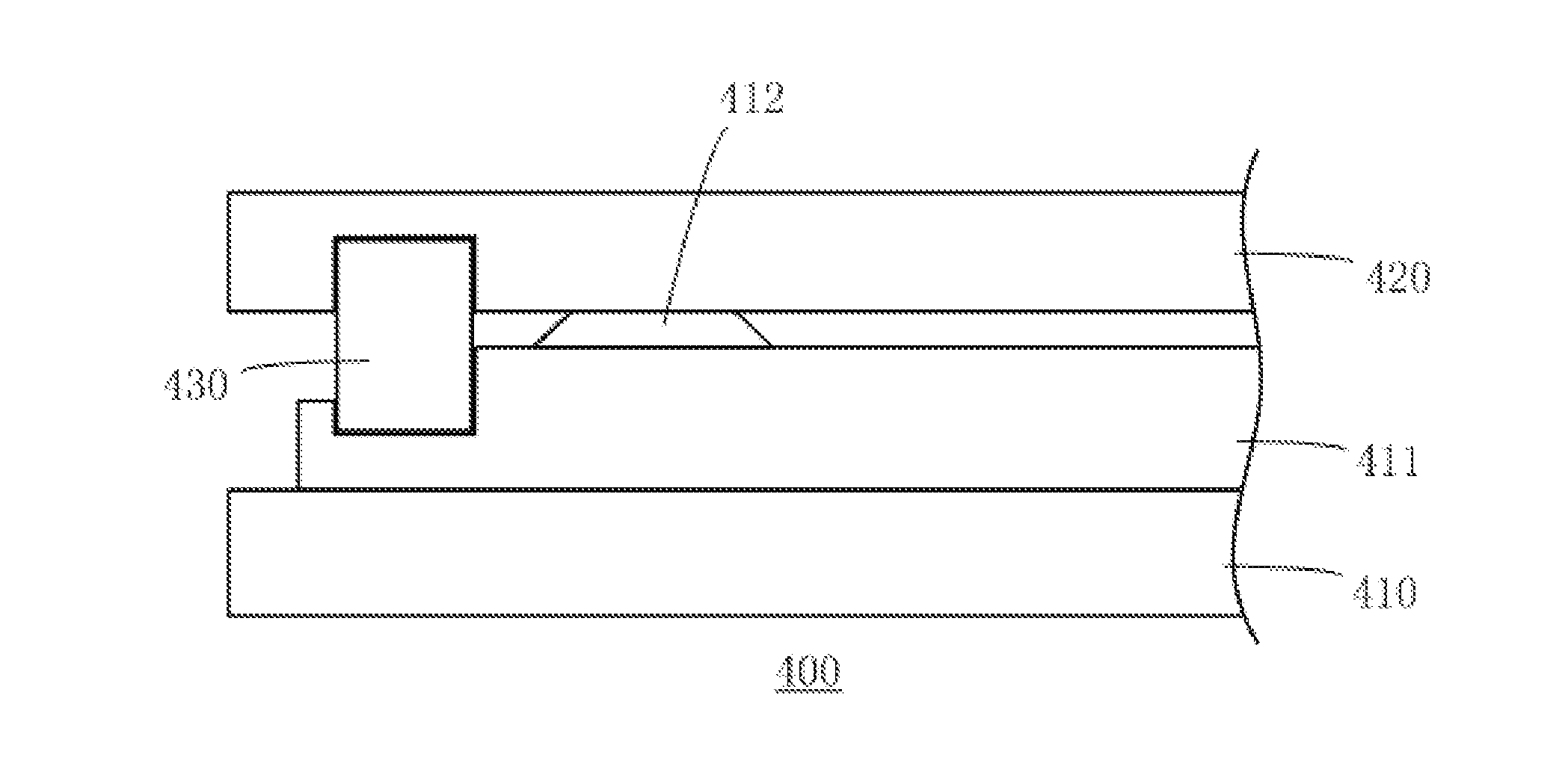
[0015]As shown in FIG. 4, an OLED package structure 400 according to an embodiment is shown. The OLED package structure 400 includes a substrate 410, a cover plate 420 and a packaging adhesive 430. On the substrate 410, an organic light-emitting element 411 including an OLED (not shown in the Figure) is provided. An annular groove is on the periphery of the inner surface of the cover plate 420 and surrounds the organic light-emitting element 411. As shown, the groove is located where the packaging adhesive 430 extends into the cover plate 420. The thickness of the packaging adhesive 430 is greater than the depth of the groove, so that a portion of the packaging adhesive 430 is in the groove of the cover plate 420, and a portion of the packaging adhesive 430 extends outside the groove of the cover plate 420. The cover plate 420 and the substrate 410 are adhered to each other by the packaging adhesive 430, so as to seal the organic light-emitting element 411.

[0016]It...

second embodiment

A Second Embodiment

[0023]A method for forming an OLED package structure, including Step S1 to Step S5 is described below. It should be noted that, in the method, the steps are named as S1 to S5 for distinguishing the steps conveniently and not for limiting the sequencing of the steps. In different embodiments according to the present invention, the sequencing of the steps may be adjusted. Steps S1 to S5 are described in conjunction with FIG. 4 to FIG. 7. The OLED package structure 400 as shown in FIG. 4 is formed with Steps S1 to S5 (corresponding to structures shown in FIG. 5 to FIG. 7) in the embodiment.

[0024]In Step S1, an entire substrate including multiple substrate units is provided. Each substrate unit includes an organic light-emitting element.

[0025]With reference to FIG. 5, the entire substrate 510 includes multiple substrate units. As shown in FIG. 5, in this embodiment, only a portion of one substrate unit of the entire substrate 510 is shown for convenience of illustrati...


PUM


Abstract

An OLED package structure includes: a substrate, on which an organic light-emitting element is provided, and a cover plate having an annular groove surrounding the organic light-emitting element thereon. A packaging adhesive, partly inside the groove and partly outside the groove, adheres the cover plate to the substrate to seal the organic light-emitting element. In the OLED package structure according to the present invention, the thickness of the spacer can be smaller, so as to eliminate color mixture during an evaporation process and to prevent a Newton ring phenomenon in the OLED package structure.

Description

CROSS-REFERENCES TO RELATED APPLICATIONS[0001]This application claims priority to Chinese patent application No. 201210567658.1 titled “ORGANIC LIGHT-EMITTING DIODE PACKAGE STRUCTURE AND METHOD FOR FORMING THE SAME” and filed with State Intellectual Property Office of PRC on Dec. 24, 2012, which is incorporated herein by reference in its entirety.FIELD OF THE INVENTION[0002]The present invention relates to display technology, and in particular to an organic light-emitting diode package structure and a method for forming the same.BACKGROUND OF THE INVENTION[0003]Organic light-emitting diode (OLED) display, which is also referred to as organic electroluminescence display (OELD), is a most promising display technology due to its advantages such as good color contrast, active light-emitting, wide viewing angle, thinness, fast response speed and low power consumption. However, in an OLED device, it is possible for an organic light-emitting layer and an electrode to fail if they encounter...

Claims


Application Information

Patent Timeline
IPC IPC(8): H01L51/52H01L51/56
CPCH01L51/56H01L51/524H10K50/8428H10K50/841H10K50/8426H10K2102/351H10K71/851H10K71/00
Inventor XIONG, ZHIYONGZHAO, BENGANGMA, XIAOJUN
Owner SHANGHAI TIANMA MICRO ELECTRONICS CO LTD
Why Eureka
Try Eureka